Category:Tetsuji YAMAGUCHI
Appearance
Tetsuji YAMAGUCHI
Executive Summary
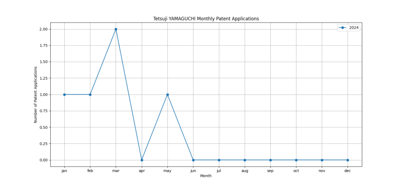
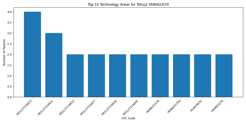
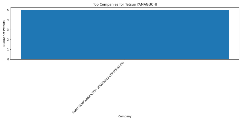
Tetsuji YAMAGUCHI is an inventor who has filed 5 patents. Their primary areas of innovation include {Optical shielding} (4 patents), {Colour filter arrangements} (3 patents), {involving a transistor} (2 patents), and they have worked with companies such as SONY SEMICONDUCTOR SOLUTIONS CORPORATION (5 patents). Their most frequent collaborators include (2 collaborations), (2 collaborations), (1 collaborations).
Patent Filing Activity
Technology Areas
List of Technology Areas
- H01L27/14623 ({Optical shielding}): 4 patents
- H01L27/14621 ({Colour filter arrangements}): 3 patents
- H01L27/14612 ({involving a transistor}): 2 patents
- H01L27/14627 ({Microlenses}): 2 patents
- H01L27/14636 ({Interconnect structures}): 2 patents
- H01L27/14645 ({Colour imagers}): 2 patents
- H04N25/134 (PICTORIAL COMMUNICATION, e.g. TELEVISION): 2 patents
- H04N25/704 (Pixels specially adapted for focusing, e.g. phase difference pixel sets): 2 patents
- H10K39/32 (ORGANIC ELECTRIC SOLID-STATE DEVICES): 2 patents
- H04N25/76 (Addressed sensors, e.g. MOS or CMOS sensors): 2 patents
- H04N23/663 (PICTORIAL COMMUNICATION, e.g. TELEVISION): 1 patents
- G02B7/34 (OPTICAL ELEMENTS, SYSTEMS OR APPARATUS): 1 patents
- H01L27/1464 ({Back illuminated imager structures}): 1 patents
- H04N23/672 (Focus control based on electronic image sensor signals): 1 patents
- H04N25/778 (comprising amplifiers shared between a plurality of pixels, i.e. at least one part of the amplifier must be on the sensor array itself): 1 patents
- H10K39/00 (Integrated devices, or assemblies of multiple devices, comprising at least one organic radiation-sensitive element covered by group): 1 patents
- H01L27/14605 ({Structural or functional details relating to the position of the pixel elements, e.g. smaller pixel elements in the center of the imager compared to pixel elements at the periphery}): 1 patents
- H01L27/14638 ({Structures specially adapted for transferring the charges across the imager perpendicular to the imaging plane}): 1 patents
- H01L27/14649 ({Infrared imagers}): 1 patents
- H10N10/13 (No explanation available): 1 patents
- G01J1/44 (Electric circuits {(for command of an exposure part): 1 patents
- H10N10/855 (No explanation available): 1 patents
- H10N10/01 (No explanation available): 1 patents
- H01L27/14632 ({Wafer-level processed structures}): 1 patents
- H01L27/14687 ({Wafer level processing}): 1 patents
- H01L29/7869 (SEMICONDUCTOR DEVICES NOT COVERED BY CLASS): 1 patents
- H01L29/24 (SEMICONDUCTOR DEVICES NOT COVERED BY CLASS): 1 patents
- H01L29/16 (SEMICONDUCTOR DEVICES NOT COVERED BY CLASS): 1 patents
- H01L27/14665 ({Imagers using a photoconductor layer}): 1 patents
- H01L27/14603 ({Special geometry or disposition of pixel-elements, address-lines or gate-electrodes}): 1 patents
- H01L27/14609 ({Pixel-elements with integrated switching, control, storage or amplification elements (scanning details of imagers (circuitry of solid-state image sensors): 1 patents
- H04N25/63 (applied to dark current): 1 patents
- H04N25/70 (SSIS architectures; Circuits associated therewith): 1 patents
- H10K19/20 (ORGANIC ELECTRIC SOLID-STATE DEVICES): 1 patents
Companies
List of Companies
- SONY SEMICONDUCTOR SOLUTIONS CORPORATION: 5 patents
Collaborators
- Keisuke HATANO (2 collaborations)
- Fumihiko KOGA (2 collaborations)
- Shinichiro IZAWA (1 collaborations)
- Hideaki TOGASHI (1 collaborations)
- Nobuhiro KAWAI (1 collaborations)
- Koji SEKIGUCHI (1 collaborations)
- Masahiro JOEI (1 collaborations)
- Kenichi MURATA (1 collaborations)
- Shintarou HIRATA (1 collaborations)
- Yuta HASEGAWA (1 collaborations)
- Yoshito NAGASHIMA (1 collaborations)
- Ryosuke NAKAMURA (1 collaborations)
- Yuji UESUGI (1 collaborations)
Subcategories
This category has the following 2 subcategories, out of 2 total.


