Category:Fumihiko KOGA
Appearance
Fumihiko KOGA
Executive Summary
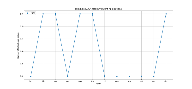
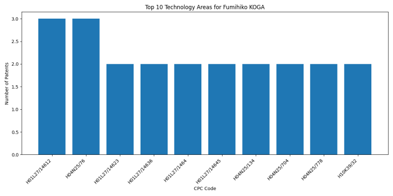
Fumihiko KOGA is an inventor who has filed 5 patents. Their primary areas of innovation include {involving a transistor} (3 patents), Addressed sensors, e.g. MOS or CMOS sensors (3 patents), {Optical shielding} (2 patents), and they have worked with companies such as SONY SEMICONDUCTOR SOLUTIONS CORPORATION (5 patents). Their most frequent collaborators include (3 collaborations), (2 collaborations), (2 collaborations).
Patent Filing Activity
Technology Areas
List of Technology Areas
- H01L27/14612 ({involving a transistor}): 3 patents
- H04N25/76 (Addressed sensors, e.g. MOS or CMOS sensors): 3 patents
- H01L27/14623 ({Optical shielding}): 2 patents
- H01L27/14636 ({Interconnect structures}): 2 patents
- H01L27/1464 ({Back illuminated imager structures}): 2 patents
- H01L27/14645 ({Colour imagers}): 2 patents
- H04N25/134 (PICTORIAL COMMUNICATION, e.g. TELEVISION): 2 patents
- H04N25/704 (Pixels specially adapted for focusing, e.g. phase difference pixel sets): 2 patents
- H04N25/778 (comprising amplifiers shared between a plurality of pixels, i.e. at least one part of the amplifier must be on the sensor array itself): 2 patents
- H10K39/32 (ORGANIC ELECTRIC SOLID-STATE DEVICES): 2 patents
- H01L27/14643 ({Photodiode arrays; MOS imagers}): 2 patents
- H04N23/663 (PICTORIAL COMMUNICATION, e.g. TELEVISION): 1 patents
- G02B7/34 (OPTICAL ELEMENTS, SYSTEMS OR APPARATUS): 1 patents
- H01L27/14621 ({Colour filter arrangements}): 1 patents
- H01L27/14627 ({Microlenses}): 1 patents
- H04N23/672 (Focus control based on electronic image sensor signals): 1 patents
- H10K39/00 (Integrated devices, or assemblies of multiple devices, comprising at least one organic radiation-sensitive element covered by group): 1 patents
- H04N25/771 (comprising storage means other than floating diffusion): 1 patents
- H01L27/14694 ({Assemblies, i.e. hybrid integration}): 1 patents
- H04N25/79 (Arrangements of circuitry being divided between different or multiple substrates, chips or circuit boards, e.g. stacked image sensors): 1 patents
- H01L27/14632 ({Wafer-level processed structures}): 1 patents
- H01L27/14687 ({Wafer level processing}): 1 patents
- H04N25/616 (involving a correlated sampling function, e.g. correlated double sampling [CDS] or triple sampling): 1 patents
- H01L27/14665 ({Imagers using a photoconductor layer}): 1 patents
- H01L27/14647 ({Multicolour imagers having a stacked pixel-element structure, e.g. npn, npnpn or MQW elements}): 1 patents
- H04N23/10 (PICTORIAL COMMUNICATION, e.g. TELEVISION): 1 patents
- H04N25/65 (applied to reset noise, e.g. KTC noise related to CMOS structures by techniques other than CDS): 1 patents
- H04N25/67 (applied to fixed-pattern noise, e.g. non-uniformity of response): 1 patents
- H04N25/68 (applied to defects): 1 patents
- H04N25/70 (SSIS architectures; Circuits associated therewith): 1 patents
- H04N25/772 (comprising A/D, V/T, V/F, I/T or I/F converters): 1 patents
Companies
List of Companies
- SONY SEMICONDUCTOR SOLUTIONS CORPORATION: 5 patents
Collaborators
- Keisuke HATANO (3 collaborations)
- Tetsuji YAMAGUCHI (2 collaborations)
- Yuji UESUGI (2 collaborations)
- Shinichiro IZAWA (1 collaborations)
- Taiichiro WATANABE (1 collaborations)
- Ryosuke NAKAMURA (1 collaborations)
Subcategories
This category has the following 2 subcategories, out of 2 total.


