Category:Chih-Hao WANG
Appearance
Chih-Hao WANG
Executive Summary
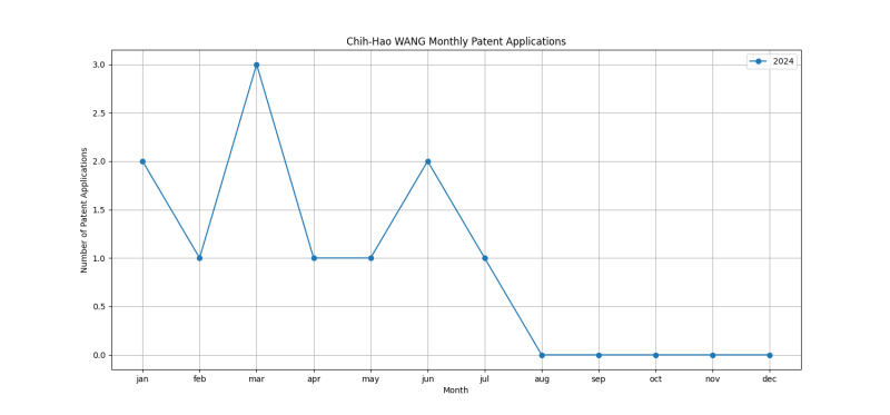
Chih-Hao WANG is an inventor who has filed 19 patents. Their primary areas of innovation include No explanation available (10 patents), No explanation available (7 patents), No explanation available (7 patents), and they have worked with companies such as TAIWAN SEMICONDUCTOR MANUFACTURING COMPANY, LTD. (9 patents), Taiwan Semiconductor Manufacturing Company, Ltd. (6 patents), Taiwan Semiconductor Manufacturing Company Ltd. (2 patents). Their most frequent collaborators include (16 collaborations), (5 collaborations), (3 collaborations).
Patent Filing Activity
Technology Areas
List of Technology Areas
- H10D84/038 (No explanation available): 10 patents
- H10D62/121 (No explanation available): 7 patents
- H10D64/017 (No explanation available): 7 patents
- H10D30/6735 (No explanation available): 6 patents
- H10D30/014 (No explanation available): 6 patents
- H10D30/43 (No explanation available): 6 patents
- H10D30/6757 (No explanation available): 6 patents
- H01L29/42392 (SEMICONDUCTOR DEVICES NOT COVERED BY CLASS): 6 patents
- H10D84/013 (No explanation available): 5 patents
- H10D84/83 (No explanation available): 5 patents
- H10D84/0151 (No explanation available): 5 patents
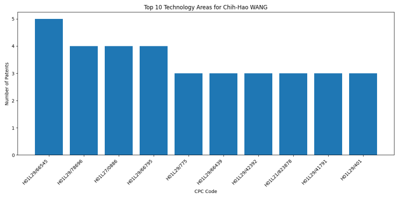
- H01L29/66545 ({using a dummy, i.e. replacement gate in a process wherein at least a part of the final gate is self aligned to the dummy gate}): 5 patents
- H01L29/78696 (SEMICONDUCTOR DEVICES NOT COVERED BY CLASS): 5 patents
- H01L29/0673 (SEMICONDUCTOR DEVICES NOT COVERED BY CLASS): 4 patents
- H01L29/66439 (SEMICONDUCTOR DEVICES NOT COVERED BY CLASS): 4 patents
- H01L29/775 (SEMICONDUCTOR DEVICES NOT COVERED BY CLASS): 4 patents
- H10D62/151 (No explanation available): 4 patents
- H10D84/0147 (No explanation available): 3 patents
- H10D84/834 (No explanation available): 3 patents
- H01L27/088 (SEMICONDUCTOR DEVICES NOT COVERED BY CLASS): 3 patents
- H10D30/62 (No explanation available): 3 patents
- H10D30/6219 (No explanation available): 3 patents
- H10D62/116 (No explanation available): 3 patents
- H10D64/018 (No explanation available): 3 patents
- H10D64/021 (No explanation available): 2 patents
- H10D84/0135 (No explanation available): 2 patents
- H01L21/76843 ({formed in openings in a dielectric}): 2 patents
- H01L21/76871 ({Layers specifically deposited to enhance or enable the nucleation of further layers, i.e. seed layers}): 2 patents
- H01L23/528 ({Geometry or} layout of the interconnection structure {(): 2 patents
- H10D84/0149 (No explanation available): 2 patents
- H10D84/0158 (No explanation available): 2 patents
- H01L21/823437 (to produce devices, e.g. integrated circuits, each consisting of a plurality of components): 2 patents
- H01L21/823481 (to produce devices, e.g. integrated circuits, each consisting of a plurality of components): 2 patents
- H01L29/41733 (SEMICONDUCTOR DEVICES NOT COVERED BY CLASS): 2 patents
- H01L21/823412 (to produce devices, e.g. integrated circuits, each consisting of a plurality of components): 2 patents
- H01L21/823418 (to produce devices, e.g. integrated circuits, each consisting of a plurality of components): 2 patents
- H01L29/0847 (SEMICONDUCTOR DEVICES NOT COVERED BY CLASS): 2 patents
- H01L2029/7858 (SEMICONDUCTOR DEVICES NOT COVERED BY CLASS): 2 patents
- H01L23/535 (including internal interconnections, e.g. cross-under constructions {(internal lead connections): 2 patents
- H10D30/0243 (No explanation available): 2 patents
- H10D62/115 (No explanation available): 2 patents
- H10D84/0167 (No explanation available): 2 patents
- H01L21/76885 ({By forming conductive members before deposition of protective insulating material, e.g. pillars, studs}): 1 patents
- H01L21/28518 (from a gas or vapour, e.g. condensation): 1 patents
- H01L29/45 (SEMICONDUCTOR DEVICES NOT COVERED BY CLASS): 1 patents
- H01L29/0665 (SEMICONDUCTOR DEVICES NOT COVERED BY CLASS): 1 patents
- H01L29/66553 ({using self aligned silicidation, i.e. salicide (formation of conductive layers comprising silicides): 1 patents
- H01L29/78651 (SEMICONDUCTOR DEVICES NOT COVERED BY CLASS): 1 patents
- H01L29/42384 (SEMICONDUCTOR DEVICES NOT COVERED BY CLASS): 1 patents
- H01L29/785 (SEMICONDUCTOR DEVICES NOT COVERED BY CLASS): 1 patents
- H01L21/76897 ({Formation of self-aligned vias or contact plugs, i.e. involving a lithographically uncritical step (self-aligned silicidation on field effect transistors): 1 patents
- H01L29/401 (SEMICONDUCTOR DEVICES NOT COVERED BY CLASS): 1 patents
- H01L21/76802 (Applying interconnections to be used for carrying current between separate components within a device {comprising conductors and dielectrics}): 1 patents
- H01L21/823468 (to produce devices, e.g. integrated circuits, each consisting of a plurality of components): 1 patents
- H01L21/823475 (to produce devices, e.g. integrated circuits, each consisting of a plurality of components): 1 patents
- H01L29/6656 ({using self aligned silicidation, i.e. salicide (formation of conductive layers comprising silicides): 1 patents
- H10D84/0128 (No explanation available): 1 patents
- H01L21/0337 ({characterised by the process involved to create the mask, e.g. lift-off masks, sidewalls, or to modify the mask, e.g. pre-treatment, post-treatment}): 1 patents
- H01L21/28088 (Manufacture of electrodes on semiconductor bodies using processes or apparatus not provided for in groups): 1 patents
- H01L21/3086 ({characterised by the process involved to create the mask, e.g. lift-off masks, sidewalls, or to modify the mask, e.g. pre-treatment, post-treatment}): 1 patents
- H10D64/667 (No explanation available): 1 patents
- H10D84/0172 (No explanation available): 1 patents
- H10D84/0184 (No explanation available): 1 patents
- H10D84/0188 (No explanation available): 1 patents
- H10D84/0193 (No explanation available): 1 patents
- H10D84/853 (No explanation available): 1 patents
- H10D30/024 (No explanation available): 1 patents
- H10D62/118 (No explanation available): 1 patents
- H10D62/83 (No explanation available): 1 patents
- H01L29/41791 (SEMICONDUCTOR DEVICES NOT COVERED BY CLASS): 1 patents
- H01L21/823814 (to produce devices, e.g. integrated circuits, each consisting of a plurality of components): 1 patents
- H01L21/823821 (to produce devices, e.g. integrated circuits, each consisting of a plurality of components): 1 patents
- H01L27/0924 (SEMICONDUCTOR DEVICES NOT COVERED BY CLASS): 1 patents
- H01L29/66795 (SEMICONDUCTOR DEVICES NOT COVERED BY CLASS): 1 patents
- H01L29/7851 (SEMICONDUCTOR DEVICES NOT COVERED BY CLASS): 1 patents
- H01L21/76895 (Applying interconnections to be used for carrying current between separate components within a device {comprising conductors and dielectrics}): 1 patents
- H01L29/456 (SEMICONDUCTOR DEVICES NOT COVERED BY CLASS): 1 patents
- H10D84/85 (No explanation available): 1 patents
Companies
List of Companies
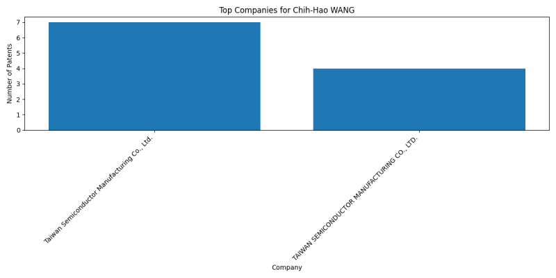
- TAIWAN SEMICONDUCTOR MANUFACTURING COMPANY, LTD.: 9 patents
- Taiwan Semiconductor Manufacturing Company, Ltd.: 6 patents
- Taiwan Semiconductor Manufacturing Company Ltd.: 2 patents
- Taiwan Semiconductor Manufacturing Company Limited: 2 patents
Collaborators
- Kuo-Cheng CHIANG (16 collaborations)
- Huan-Chieh SU (5 collaborations)
- Lung-Kun CHU (3 collaborations)
- Jia-Ni YU (3 collaborations)
- Chung-Wei HSU (3 collaborations)
- Jia-Chuan YOU (3 collaborations)
- Kuan-Ting PAN (3 collaborations)
- Chun-Yuan CHEN (3 collaborations)
- Guan-Lin CHEN (3 collaborations)
- Shi Ning JU (3 collaborations)
- Chun-Fu LU (2 collaborations)
- Shih-Hao LAI (2 collaborations)
- Shi-Ning JU (2 collaborations)
- Chia-Hao CHANG (2 collaborations)
- Chun Yi CHOU (2 collaborations)
- Kuan-Lun CHENG (2 collaborations)
- Jung-Hung CHANG (2 collaborations)
- Tsung-Han CHUANG (2 collaborations)
- Fu-Cheng CHANG (2 collaborations)
- Shih-Cheng CHEN (2 collaborations)
- Chia-Cheng TSAI (2 collaborations)
- Sheng-Tsung WANG (2 collaborations)
- Szu-Chien WU (1 collaborations)
- Shang-Wen CHANG (1 collaborations)
- Ching-Wei TSAI (1 collaborations)
- Chu-Yuan HSU (1 collaborations)
- Chun-Hsiung LIN (1 collaborations)
- Pei-Hsun WANG (1 collaborations)
- Kuo-Cheng CHING (1 collaborations)
- Jui-Chien HUANG (1 collaborations)
- Mao-Lin HUANG (1 collaborations)
- Wen-Ting LAN (1 collaborations)
- Wang-Chun Huang (1 collaborations)
- Shi-Syuan Huang (1 collaborations)
- Min-Hsuan LU (1 collaborations)
- Tzu Pei CHEN (1 collaborations)
- Hao-Heng LIU (1 collaborations)
- Chien-Hung LIN (1 collaborations)
- Lo-Heng CHANG (1 collaborations)
- Li-Zhen Yu (1 collaborations)
- Chia-Hao Chang (1 collaborations)
- Lin-Yu Huang (1 collaborations)
- Cheng-Chi Chuang (1 collaborations)
Subcategories
This category has the following 4 subcategories, out of 4 total.
Categories:
- Kuo-Cheng CHIANG
- Huan-Chieh SU
- Lung-Kun CHU
- Jia-Ni YU
- Chung-Wei HSU
- Jia-Chuan YOU
- Kuan-Ting PAN
- Chun-Yuan CHEN
- Guan-Lin CHEN
- Shi Ning JU
- Chun-Fu LU
- Shih-Hao LAI
- Shi-Ning JU
- Chia-Hao CHANG
- Chun Yi CHOU
- Kuan-Lun CHENG
- Jung-Hung CHANG
- Tsung-Han CHUANG
- Fu-Cheng CHANG
- Shih-Cheng CHEN
- Chia-Cheng TSAI
- Sheng-Tsung WANG
- Szu-Chien WU
- Shang-Wen CHANG
- Ching-Wei TSAI
- Chu-Yuan HSU
- Chun-Hsiung LIN
- Pei-Hsun WANG
- Kuo-Cheng CHING
- Jui-Chien HUANG
- Mao-Lin HUANG
- Wen-Ting LAN
- Wang-Chun Huang
- Shi-Syuan Huang
- Min-Hsuan LU
- Tzu Pei CHEN
- Hao-Heng LIU
- Chien-Hung LIN
- Lo-Heng CHANG
- Li-Zhen Yu
- Chia-Hao Chang
- Lin-Yu Huang
- Cheng-Chi Chuang
- Chih-Hao WANG
- Inventors
- Inventors filing patents with TAIWAN SEMICONDUCTOR MANUFACTURING COMPANY, LTD.
- Inventors filing patents with Taiwan Semiconductor Manufacturing Company, Ltd.
- Inventors filing patents with Taiwan Semiconductor Manufacturing Company Ltd.
- Inventors filing patents with Taiwan Semiconductor Manufacturing Company Limited


