Category:Chung-Shi Liu
Appearance
Chung-Shi Liu
Executive Summary
Chung-Shi Liu is an inventor who has filed 11 patents. Their primary areas of innovation include Leads, {i.e. metallisations or lead-frames} on insulating substrates, {e.g. chip carriers (shape of the substrate (3 patents), {Multilayer substrates (multilayer metallisation on monolayer substrate (3 patents), SEMICONDUCTOR DEVICES NOT COVERED BY CLASS (2 patents), and they have worked with companies such as Taiwan Semiconductor Manufacturing Company, Ltd. (9 patents), Taiwan Semiconductor Manufacturing Company Limited (2 patents). Their most frequent collaborators include (10 collaborations), (4 collaborations), (3 collaborations).
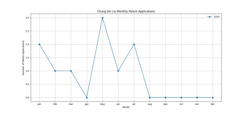
Patent Filing Activity
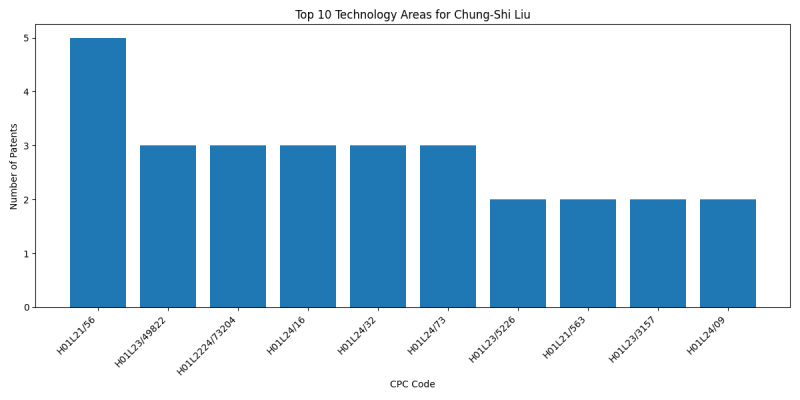
Technology Areas
List of Technology Areas
- H01L23/49838 (Leads, {i.e. metallisations or lead-frames} on insulating substrates, {e.g. chip carriers (shape of the substrate): 3 patents
- H01L23/49822 ({Multilayer substrates (multilayer metallisation on monolayer substrate): 3 patents
- H01L24/16 (SEMICONDUCTOR DEVICES NOT COVERED BY CLASS): 2 patents
- H01L23/5386 (the interconnection structure between a plurality of semiconductor chips being formed on, or in, insulating substrates ({): 2 patents
- H01L23/49816 (Leads, {i.e. metallisations or lead-frames} on insulating substrates, {e.g. chip carriers (shape of the substrate): 2 patents
- H01L25/0655 (SEMICONDUCTOR DEVICES NOT COVERED BY CLASS): 2 patents
- H01L21/76254 (Dielectric regions {, e.g. EPIC dielectric isolation, LOCOS; Trench refilling techniques, SOI technology, use of channel stoppers}): 2 patents
- H01L24/17 (SEMICONDUCTOR DEVICES NOT COVERED BY CLASS): 2 patents
- H05K1/0298 (PRINTED CIRCUITS; CASINGS OR CONSTRUCTIONAL DETAILS OF ELECTRIC APPARATUS; MANUFACTURE OF ASSEMBLAGES OF ELECTRICAL COMPONENTS): 2 patents
- H01L23/3128 (SEMICONDUCTOR DEVICES NOT COVERED BY CLASS): 2 patents
- G02B6/4202 (Coupling light guides with opto-electronic elements): 1 patents
- G02B6/4274 (Coupling light guides with opto-electronic elements): 1 patents
- H01L21/7684 (Applying interconnections to be used for carrying current between separate components within a device {comprising conductors and dielectrics}): 1 patents
- H01L2224/16055 (SEMICONDUCTOR DEVICES NOT COVERED BY CLASS): 1 patents
- H01L2224/16112 (SEMICONDUCTOR DEVICES NOT COVERED BY CLASS): 1 patents
- H01L2224/16148 (SEMICONDUCTOR DEVICES NOT COVERED BY CLASS): 1 patents
- H01L2924/19033 (SEMICONDUCTOR DEVICES NOT COVERED BY CLASS): 1 patents
- G02B6/4283 (Coupling light guides with opto-electronic elements): 1 patents
- G02B6/4291 (Coupling light guides with opto-electronic elements): 1 patents
- G02B6/4293 (Coupling light guides with opto-electronic elements): 1 patents
- H01L23/49833 (Leads, {i.e. metallisations or lead-frames} on insulating substrates, {e.g. chip carriers (shape of the substrate): 1 patents
- H01L23/5385 (the interconnection structure between a plurality of semiconductor chips being formed on, or in, insulating substrates ({): 1 patents
- H01L2224/16235 (SEMICONDUCTOR DEVICES NOT COVERED BY CLASS): 1 patents
- H01L2924/1434 (SEMICONDUCTOR DEVICES NOT COVERED BY CLASS): 1 patents
- H01L2924/1811 (SEMICONDUCTOR DEVICES NOT COVERED BY CLASS): 1 patents
- H01L2924/182 (SEMICONDUCTOR DEVICES NOT COVERED BY CLASS): 1 patents
- G02B6/4214 (Coupling light guides with opto-electronic elements): 1 patents
- H01L21/266 (using masks {(): 1 patents
- G02F1/0113 ({in optical waveguides, not otherwise provided for in this subclass}): 1 patents
- G02F1/0102 (for the control of the intensity, phase, polarisation or colour (): 1 patents
- G02F2201/02 (OPTICAL DEVICES OR ARRANGEMENTS FOR THE CONTROL OF LIGHT BY MODIFICATION OF THE OPTICAL PROPERTIES OF THE MEDIA OF THE ELEMENTS INVOLVED THEREIN; NON-LINEAR OPTICS; FREQUENCY-CHANGING OF LIGHT; OPTICAL LOGIC ELEMENTS; OPTICAL ANALOGUE/DIGITAL CONVERTERS): 1 patents
- G02F2201/128 (OPTICAL DEVICES OR ARRANGEMENTS FOR THE CONTROL OF LIGHT BY MODIFICATION OF THE OPTICAL PROPERTIES OF THE MEDIA OF THE ELEMENTS INVOLVED THEREIN; NON-LINEAR OPTICS; FREQUENCY-CHANGING OF LIGHT; OPTICAL LOGIC ELEMENTS; OPTICAL ANALOGUE/DIGITAL CONVERTERS): 1 patents
- G02F2201/302 (OPTICAL DEVICES OR ARRANGEMENTS FOR THE CONTROL OF LIGHT BY MODIFICATION OF THE OPTICAL PROPERTIES OF THE MEDIA OF THE ELEMENTS INVOLVED THEREIN; NON-LINEAR OPTICS; FREQUENCY-CHANGING OF LIGHT; OPTICAL LOGIC ELEMENTS; OPTICAL ANALOGUE/DIGITAL CONVERTERS): 1 patents
- H01L24/83 (SEMICONDUCTOR DEVICES NOT COVERED BY CLASS): 1 patents
- H01L2224/83896 (SEMICONDUCTOR DEVICES NOT COVERED BY CLASS): 1 patents
- H01L23/3185 (SEMICONDUCTOR DEVICES NOT COVERED BY CLASS): 1 patents
- H01L23/5226 (SEMICONDUCTOR DEVICES NOT COVERED BY CLASS): 1 patents
- H01L23/5283 ({Geometry or} layout of the interconnection structure {(): 1 patents
- H01L23/53228 (SEMICONDUCTOR DEVICES NOT COVERED BY CLASS): 1 patents
- H01L23/5383 ({Multilayer substrates (): 1 patents
- H01L24/09 (SEMICONDUCTOR DEVICES NOT COVERED BY CLASS): 1 patents
- H01L25/50 ({Multistep manufacturing processes of assemblies consisting of devices, each device being of a type provided for in group): 1 patents
- H05K1/0271 (PRINTED CIRCUITS; CASINGS OR CONSTRUCTIONAL DETAILS OF ELECTRIC APPARATUS; MANUFACTURE OF ASSEMBLAGES OF ELECTRICAL COMPONENTS): 1 patents
- H01L2224/02373 (SEMICONDUCTOR DEVICES NOT COVERED BY CLASS): 1 patents
- H01L24/20 (SEMICONDUCTOR DEVICES NOT COVERED BY CLASS): 1 patents
- H01L21/565 (SEMICONDUCTOR DEVICES NOT COVERED BY CLASS): 1 patents
- H01L21/568 (SEMICONDUCTOR DEVICES NOT COVERED BY CLASS): 1 patents
- H01L23/4006 (SEMICONDUCTOR DEVICES NOT COVERED BY CLASS): 1 patents
- H01L24/19 (SEMICONDUCTOR DEVICES NOT COVERED BY CLASS): 1 patents
- H01L2023/4031 (SEMICONDUCTOR DEVICES NOT COVERED BY CLASS): 1 patents
- H01L2023/405 (SEMICONDUCTOR DEVICES NOT COVERED BY CLASS): 1 patents
- H01L2023/4087 (SEMICONDUCTOR DEVICES NOT COVERED BY CLASS): 1 patents
- H01L2224/211 (SEMICONDUCTOR DEVICES NOT COVERED BY CLASS): 1 patents
- H01L23/3135 (SEMICONDUCTOR DEVICES NOT COVERED BY CLASS): 1 patents
- H01L21/563 (SEMICONDUCTOR DEVICES NOT COVERED BY CLASS): 1 patents
- H01L23/3142 (SEMICONDUCTOR DEVICES NOT COVERED BY CLASS): 1 patents
- H01L2224/02335 (SEMICONDUCTOR DEVICES NOT COVERED BY CLASS): 1 patents
- H01L2224/12105 (SEMICONDUCTOR DEVICES NOT COVERED BY CLASS): 1 patents
- H05K3/4046 (PRINTED CIRCUITS; CASINGS OR CONSTRUCTIONAL DETAILS OF ELECTRIC APPARATUS; MANUFACTURE OF ASSEMBLAGES OF ELECTRICAL COMPONENTS): 1 patents
- H01L23/3735 (SEMICONDUCTOR DEVICES NOT COVERED BY CLASS): 1 patents
- H01L23/5384 ({Conductive vias through the substrate with or without pins, e.g. buried coaxial conductors (): 1 patents
- H05K1/113 (PRINTED CIRCUITS; CASINGS OR CONSTRUCTIONAL DETAILS OF ELECTRIC APPARATUS; MANUFACTURE OF ASSEMBLAGES OF ELECTRICAL COMPONENTS): 1 patents
- H05K3/0061 (Apparatus or processes for manufacturing printed circuits): 1 patents
- Y10T29/49165 (No explanation available): 1 patents
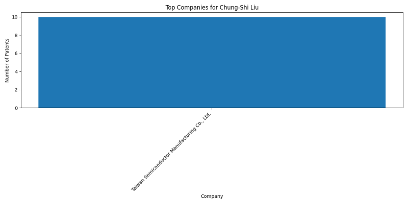
Companies
List of Companies
- Taiwan Semiconductor Manufacturing Company, Ltd.: 9 patents
- Taiwan Semiconductor Manufacturing Company Limited: 2 patents
Collaborators
- Chen-Hua Yu (10 collaborations)
- Hao-Yi Tsai (4 collaborations)
- Tsung-Fu Tsai (3 collaborations)
- Szu-Wei Lu (3 collaborations)
- Jiun-Yi Wu (3 collaborations)
- Chung-Ming Weng (2 collaborations)
- Cheng-Chieh Hsieh (2 collaborations)
- Hung-Yi Kuo (2 collaborations)
- Tsung-Yuan Yu (2 collaborations)
- Hua-Kuei Lin (2 collaborations)
- Chien-Hsun Lee (2 collaborations)
- Jih-Churng Twu (2 collaborations)
- Tin-Hao Kuo (2 collaborations)
- Hsiu-Jen Lin (1 collaborations)
- Ming-Che Ho (1 collaborations)
- Yu-Hsiang Hu (1 collaborations)
- Chewn-Pu Jou (1 collaborations)
- Cheng-Tse Tang (1 collaborations)
- Chao-Jen Wang (1 collaborations)
- Chien-Hsun Chen (1 collaborations)
- Shou-Yi Wang (1 collaborations)
- Tsung-Ding Wang (1 collaborations)
- Che-Hsiang Hsu (1 collaborations)
- Su-Chun Yang (1 collaborations)
- Jui Hsuan Tsai (1 collaborations)
- Shuen-Shin Liang (1 collaborations)
- Chen-Chiang Yu (1 collaborations)
- Yu-Chia Lai (1 collaborations)
- Po-Yuan Teng (1 collaborations)
- Yu-Min Liang (1 collaborations)
Subcategories
This category has the following 10 subcategories, out of 10 total.
C
H
J
K
S
W
Categories:
- Chen-Hua Yu
- Hao-Yi Tsai
- Tsung-Fu Tsai
- Szu-Wei Lu
- Jiun-Yi Wu
- Chung-Ming Weng
- Cheng-Chieh Hsieh
- Hung-Yi Kuo
- Tsung-Yuan Yu
- Hua-Kuei Lin
- Chien-Hsun Lee
- Jih-Churng Twu
- Tin-Hao Kuo
- Hsiu-Jen Lin
- Ming-Che Ho
- Yu-Hsiang Hu
- Chewn-Pu Jou
- Cheng-Tse Tang
- Chao-Jen Wang
- Chien-Hsun Chen
- Shou-Yi Wang
- Tsung-Ding Wang
- Che-Hsiang Hsu
- Su-Chun Yang
- Jui Hsuan Tsai
- Shuen-Shin Liang
- Chen-Chiang Yu
- Yu-Chia Lai
- Po-Yuan Teng
- Yu-Min Liang
- Chung-Shi Liu
- Inventors
- Inventors filing patents with Taiwan Semiconductor Manufacturing Company, Ltd.
- Inventors filing patents with Taiwan Semiconductor Manufacturing Company Limited


