Category:Ming-Fa Chen
Appearance
Ming-Fa Chen
Executive Summary
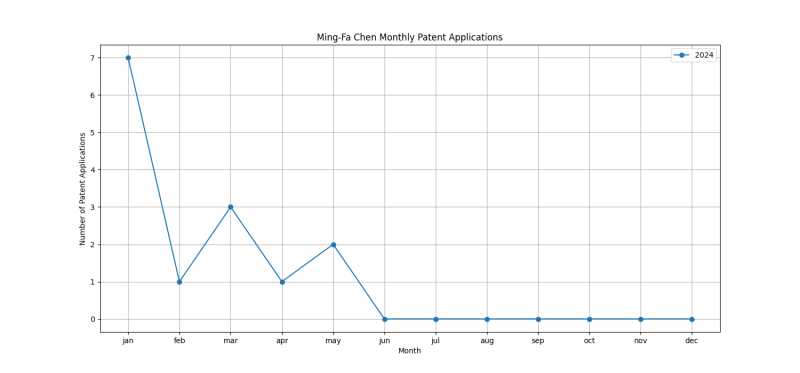
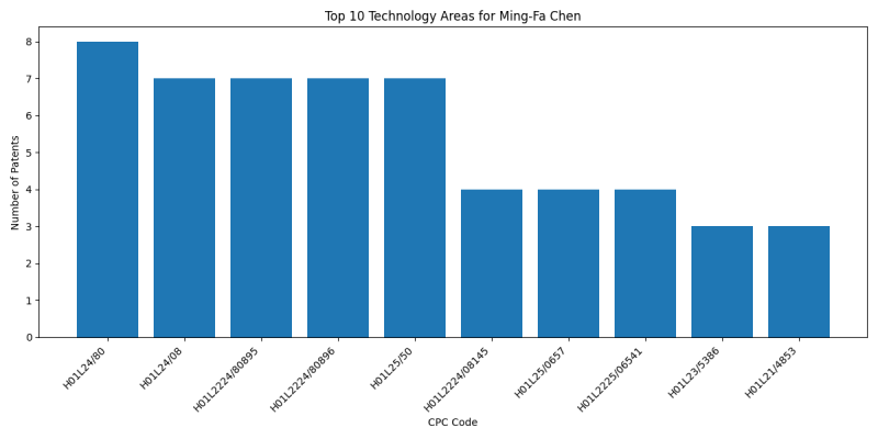
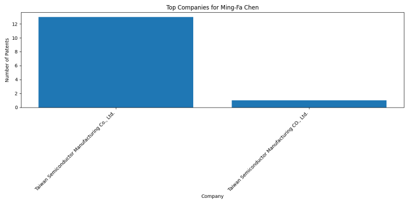
Ming-Fa Chen is an inventor who has filed 14 patents. Their primary areas of innovation include {Methods for connecting semiconductor or other solid state bodies using means for bonding being attached to, or being formed on, the surface to be connected} (8 patents), SEMICONDUCTOR DEVICES NOT COVERED BY CLASS (7 patents), SEMICONDUCTOR DEVICES NOT COVERED BY CLASS (7 patents), and they have worked with companies such as Taiwan Semiconductor Manufacturing Co., Ltd. (13 patents), Taiwan Semiconductor Manufacturing CO., Ltd. (1 patents). Their most frequent collaborators include (6 collaborations), (3 collaborations), (3 collaborations).
Patent Filing Activity
Technology Areas
List of Technology Areas
- H01L24/80 ({Methods for connecting semiconductor or other solid state bodies using means for bonding being attached to, or being formed on, the surface to be connected}): 8 patents
- H01L24/08 (SEMICONDUCTOR DEVICES NOT COVERED BY CLASS): 7 patents
- H01L2224/80895 (SEMICONDUCTOR DEVICES NOT COVERED BY CLASS): 7 patents
- H01L2224/80896 (SEMICONDUCTOR DEVICES NOT COVERED BY CLASS): 7 patents
- H01L25/50 ({Multistep manufacturing processes of assemblies consisting of devices, each device being of a type provided for in group): 7 patents
- H01L2224/08145 (SEMICONDUCTOR DEVICES NOT COVERED BY CLASS): 4 patents
- H01L25/0657 (SEMICONDUCTOR DEVICES NOT COVERED BY CLASS): 4 patents
- H01L2225/06541 (SEMICONDUCTOR DEVICES NOT COVERED BY CLASS): 4 patents
- H01L23/5386 (the interconnection structure between a plurality of semiconductor chips being formed on, or in, insulating substrates ({): 3 patents
- H01L21/4853 (Manufacture or treatment of parts, e.g. containers, prior to assembly of the devices, using processes not provided for in a single one of the subgroups): 3 patents
- H01L23/49816 (Leads, {i.e. metallisations or lead-frames} on insulating substrates, {e.g. chip carriers (shape of the substrate): 3 patents
- H01L25/0655 (SEMICONDUCTOR DEVICES NOT COVERED BY CLASS): 3 patents
- H01L2224/08225 (SEMICONDUCTOR DEVICES NOT COVERED BY CLASS): 3 patents
- H01L23/5389 (the interconnection structure between a plurality of semiconductor chips being formed on, or in, insulating substrates ({): 3 patents
- H01L23/49827 ({Via connections through the substrates, e.g. pins going through the substrate, coaxial cables (): 3 patents
- H01L25/0652 (SEMICONDUCTOR DEVICES NOT COVERED BY CLASS): 3 patents
- H01L25/18 (the devices being of types provided for in two or more different subgroups of the same main group of groups): 3 patents
- H01L21/565 (SEMICONDUCTOR DEVICES NOT COVERED BY CLASS): 3 patents
- H01L23/3128 (SEMICONDUCTOR DEVICES NOT COVERED BY CLASS): 3 patents
- H01L23/5385 (the interconnection structure between a plurality of semiconductor chips being formed on, or in, insulating substrates ({): 2 patents
- H01L2224/94 (SEMICONDUCTOR DEVICES NOT COVERED BY CLASS): 2 patents
- H01L2924/182 (SEMICONDUCTOR DEVICES NOT COVERED BY CLASS): 2 patents
- H01L23/5226 (SEMICONDUCTOR DEVICES NOT COVERED BY CLASS): 2 patents
- H01L24/09 (SEMICONDUCTOR DEVICES NOT COVERED BY CLASS): 2 patents
- H01L2224/08146 (SEMICONDUCTOR DEVICES NOT COVERED BY CLASS): 2 patents
- H01L21/6835 ({using temporarily an auxiliary support}): 2 patents
- H01L24/16 (SEMICONDUCTOR DEVICES NOT COVERED BY CLASS): 2 patents
- H01L2225/06524 (SEMICONDUCTOR DEVICES NOT COVERED BY CLASS): 2 patents
- H01L2225/06589 (SEMICONDUCTOR DEVICES NOT COVERED BY CLASS): 2 patents
- H01L2225/06586 (SEMICONDUCTOR DEVICES NOT COVERED BY CLASS): 2 patents
- H01L23/481 (Arrangements for conducting electric current to or from the solid state body in operation, e.g. leads, terminal arrangements {; Selection of materials therefor}): 2 patents
- H01L25/105 (SEMICONDUCTOR DEVICES NOT COVERED BY CLASS): 2 patents
- H01L2225/1035 (SEMICONDUCTOR DEVICES NOT COVERED BY CLASS): 2 patents
- H01L2225/1058 (SEMICONDUCTOR DEVICES NOT COVERED BY CLASS): 2 patents
- H01L21/4857 (Manufacture or treatment of parts, e.g. containers, prior to assembly of the devices, using processes not provided for in a single one of the subgroups): 2 patents
- H01L23/5383 ({Multilayer substrates (): 2 patents
- H01L21/82 (to produce devices, e.g. integrated circuits, each consisting of a plurality of components): 1 patents
- H01L23/5381 (the interconnection structure between a plurality of semiconductor chips being formed on, or in, insulating substrates ({): 1 patents
- H01L24/94 (SEMICONDUCTOR DEVICES NOT COVERED BY CLASS): 1 patents
- H01L2224/80203 (SEMICONDUCTOR DEVICES NOT COVERED BY CLASS): 1 patents
- H01L23/5286 ({Geometry or} layout of the interconnection structure {(): 1 patents
- H01L2224/08135 (SEMICONDUCTOR DEVICES NOT COVERED BY CLASS): 1 patents
- H01L2224/08137 (SEMICONDUCTOR DEVICES NOT COVERED BY CLASS): 1 patents
- H01L2224/08147 (SEMICONDUCTOR DEVICES NOT COVERED BY CLASS): 1 patents
- H01L21/563 (SEMICONDUCTOR DEVICES NOT COVERED BY CLASS): 1 patents
- H01L23/147 ({Semiconductor insulating substrates (semiconductor conductive substrates): 1 patents
- H01L23/3121 (SEMICONDUCTOR DEVICES NOT COVERED BY CLASS): 1 patents
- H01L23/49822 ({Multilayer substrates (multilayer metallisation on monolayer substrate): 1 patents
- H01L24/81 (SEMICONDUCTOR DEVICES NOT COVERED BY CLASS): 1 patents
- H01L24/97 (SEMICONDUCTOR DEVICES NOT COVERED BY CLASS): 1 patents
- H01L23/3677 (Cooling facilitated by shape of device {(): 1 patents
- H01L24/32 (SEMICONDUCTOR DEVICES NOT COVERED BY CLASS): 1 patents
- H01L24/73 (SEMICONDUCTOR DEVICES NOT COVERED BY CLASS): 1 patents
- H01L21/4882 (Manufacture or treatment of parts, e.g. containers, prior to assembly of the devices, using processes not provided for in a single one of the subgroups): 1 patents
- H01L2225/06517 (SEMICONDUCTOR DEVICES NOT COVERED BY CLASS): 1 patents
- H01L2924/16251 (SEMICONDUCTOR DEVICES NOT COVERED BY CLASS): 1 patents
- H01L2924/1632 (SEMICONDUCTOR DEVICES NOT COVERED BY CLASS): 1 patents
- H01L2224/16227 (SEMICONDUCTOR DEVICES NOT COVERED BY CLASS): 1 patents
- H01L2224/16237 (SEMICONDUCTOR DEVICES NOT COVERED BY CLASS): 1 patents
- H01L2224/32225 (SEMICONDUCTOR DEVICES NOT COVERED BY CLASS): 1 patents
- H01L2224/73204 (SEMICONDUCTOR DEVICES NOT COVERED BY CLASS): 1 patents
- H01L2224/08245 (SEMICONDUCTOR DEVICES NOT COVERED BY CLASS): 1 patents
- H01L2224/8083 (SEMICONDUCTOR DEVICES NOT COVERED BY CLASS): 1 patents
- H01L21/76224 ({using trench refilling with dielectric materials (trench filling with polycristalline silicon): 1 patents
- H01L21/7684 (Applying interconnections to be used for carrying current between separate components within a device {comprising conductors and dielectrics}): 1 patents
- H01L21/76846 ({Layer combinations}): 1 patents
- H01L23/585 ({comprising conductive layers or plates or strips or rods or rings (): 1 patents
- H01L23/53295 (SEMICONDUCTOR DEVICES NOT COVERED BY CLASS): 1 patents
- H01L29/0649 (SEMICONDUCTOR DEVICES NOT COVERED BY CLASS): 1 patents
- H01L24/83 (SEMICONDUCTOR DEVICES NOT COVERED BY CLASS): 1 patents
- H01L24/03 (SEMICONDUCTOR DEVICES NOT COVERED BY CLASS): 1 patents
- H01L24/33 (SEMICONDUCTOR DEVICES NOT COVERED BY CLASS): 1 patents
- H01L23/562 (SEMICONDUCTOR DEVICES NOT COVERED BY CLASS): 1 patents
- H01L2225/06568 (SEMICONDUCTOR DEVICES NOT COVERED BY CLASS): 1 patents
- H01L2225/06565 (SEMICONDUCTOR DEVICES NOT COVERED BY CLASS): 1 patents
- H01L2225/06593 (SEMICONDUCTOR DEVICES NOT COVERED BY CLASS): 1 patents
- H01L2225/06513 (SEMICONDUCTOR DEVICES NOT COVERED BY CLASS): 1 patents
- H01L2924/1434 (SEMICONDUCTOR DEVICES NOT COVERED BY CLASS): 1 patents
- H01L2924/1431 (SEMICONDUCTOR DEVICES NOT COVERED BY CLASS): 1 patents
- H01L21/76898 ({formed through a semiconductor substrate}): 1 patents
- H01L21/568 (SEMICONDUCTOR DEVICES NOT COVERED BY CLASS): 1 patents
- H01L2221/68372 (SEMICONDUCTOR DEVICES NOT COVERED BY CLASS): 1 patents
- H01L2225/06548 (SEMICONDUCTOR DEVICES NOT COVERED BY CLASS): 1 patents
- H01L2224/80006 (SEMICONDUCTOR DEVICES NOT COVERED BY CLASS): 1 patents
- H01L2225/06582 (SEMICONDUCTOR DEVICES NOT COVERED BY CLASS): 1 patents
- H01L21/481 (Manufacture or treatment of parts, e.g. containers, prior to assembly of the devices, using processes not provided for in a single one of the subgroups): 1 patents
- H01L21/56 (SEMICONDUCTOR DEVICES NOT COVERED BY CLASS): 1 patents
- H01L2225/1041 (SEMICONDUCTOR DEVICES NOT COVERED BY CLASS): 1 patents
- H01L21/4871 (Manufacture or treatment of parts, e.g. containers, prior to assembly of the devices, using processes not provided for in a single one of the subgroups): 1 patents
- H01L21/78 (with subsequent division of the substrate into plural individual devices (cutting to change the surface-physical characteristics or shape of semiconductor bodies): 1 patents
- H01L22/12 ({for structural parameters, e.g. thickness, line width, refractive index, temperature, warp, bond strength, defects, optical inspection, electrical measurement of structural dimensions, metallurgic measurement of diffusions (electrical measurement of diffusions): 1 patents
- H01L23/3675 (Cooling facilitated by shape of device {(): 1 patents
- H01L24/19 (SEMICONDUCTOR DEVICES NOT COVERED BY CLASS): 1 patents
- H01L24/20 (SEMICONDUCTOR DEVICES NOT COVERED BY CLASS): 1 patents
- H01L2224/214 (SEMICONDUCTOR DEVICES NOT COVERED BY CLASS): 1 patents
- H01L2924/19103 (SEMICONDUCTOR DEVICES NOT COVERED BY CLASS): 1 patents
- H01L24/06 ({of a plurality of bonding areas}): 1 patents
- H01L23/49503 (Lead-frames {or other flat leads (): 1 patents
- H03K19/1776 (PULSE TECHNIQUE (measuring pulse characteristics): 1 patents
- H01L23/49844 (Leads, {i.e. metallisations or lead-frames} on insulating substrates, {e.g. chip carriers (shape of the substrate): 1 patents
- H01L23/42 (Fillings or auxiliary members in containers {or encapsulations} selected or arranged to facilitate heating or cooling): 1 patents
Companies
List of Companies
- Taiwan Semiconductor Manufacturing Co., Ltd.: 13 patents
- Taiwan Semiconductor Manufacturing CO., Ltd.: 1 patents
Collaborators
- Hsien-Wei Chen (6 collaborations)
- Chen-Hua Yu (3 collaborations)
- Chih-Chia Hu (3 collaborations)
- Yun-Han Lee (2 collaborations)
- Lee-Chung Lu (2 collaborations)
- Sen-Bor Jan (2 collaborations)
- Chao-Wen Shih (2 collaborations)
- Sung-Feng Yeh (2 collaborations)
- Jie Chen (2 collaborations)
- Fong-Yuan Chang (1 collaborations)
- Noor Mohamed Ettuveettil (1 collaborations)
- Po-Hsiang Huang (1 collaborations)
- Chin-Chou Liu (1 collaborations)
- Yi-Kan Cheng (1 collaborations)
- Hsien-Pin Hu (1 collaborations)
- Jing-Cheng Lin (1 collaborations)
- Jiun Ren Lai (1 collaborations)
- Yung-Chi Lin (1 collaborations)
- Chin-Shyh Wang (1 collaborations)
- Chun-Chiang Kuo (1 collaborations)
- Ying-Ju Chen (1 collaborations)
- Chuan-An Cheng (1 collaborations)
- Tzuan-Horng Liu (1 collaborations)
Subcategories
This category has the following 2 subcategories, out of 2 total.
H
M
Categories:
- Hsien-Wei Chen
- Chen-Hua Yu
- Chih-Chia Hu
- Yun-Han Lee
- Lee-Chung Lu
- Sen-Bor Jan
- Chao-Wen Shih
- Sung-Feng Yeh
- Jie Chen
- Fong-Yuan Chang
- Noor Mohamed Ettuveettil
- Po-Hsiang Huang
- Chin-Chou Liu
- Yi-Kan Cheng
- Hsien-Pin Hu
- Jing-Cheng Lin
- Jiun Ren Lai
- Yung-Chi Lin
- Chin-Shyh Wang
- Chun-Chiang Kuo
- Ying-Ju Chen
- Chuan-An Cheng
- Tzuan-Horng Liu
- Ming-Fa Chen
- Inventors
- Inventors filing patents with Taiwan Semiconductor Manufacturing Co., Ltd.
- Inventors filing patents with Taiwan Semiconductor Manufacturing CO., Ltd.


