Category:Ming-Fa Chen: Difference between revisions
Updating Category:Ming-Fa_Chen |
Wikipatents (talk | contribs) Updating Category:Ming-Fa_Chen |
||
| Line 2: | Line 2: | ||
=== Executive Summary === | === Executive Summary === | ||
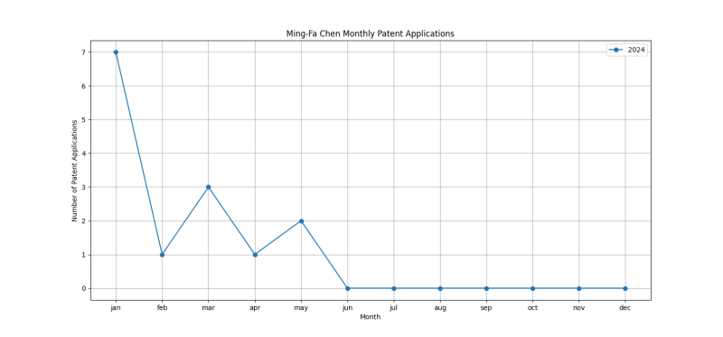
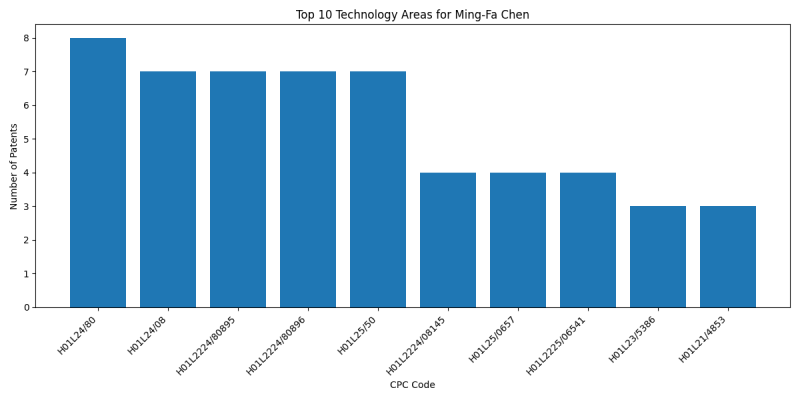
Ming-Fa Chen is an inventor who has filed | Ming-Fa Chen is an inventor who has filed 11 patents. Their primary areas of innovation include SEMICONDUCTOR DEVICES NOT COVERED BY CLASS (6 patents), SEMICONDUCTOR DEVICES NOT COVERED BY CLASS (5 patents), {Multistep manufacturing processes of assemblies consisting of devices, each device being of a type provided for in group (4 patents), and they have worked with companies such as Taiwan Semiconductor Manufacturing Company, Ltd. (11 patents). Their most frequent collaborators include [[Category:Hsien-Wei Chen|Hsien-Wei Chen]] (8 collaborations), [[Category:Jie Chen|Jie Chen]] (5 collaborations), [[Category:Sung-Feng Yeh|Sung-Feng Yeh]] (3 collaborations). | ||
=== Patent Filing Activity === | === Patent Filing Activity === | ||
| Line 11: | Line 11: | ||
==== List of Technology Areas ==== | ==== List of Technology Areas ==== | ||
* [[:Category:CPC_H01L25/0657|H01L25/0657]] (SEMICONDUCTOR DEVICES NOT COVERED BY CLASS): 4 patents | * [[:Category:CPC_H01L25/0657|H01L25/0657]] (SEMICONDUCTOR DEVICES NOT COVERED BY CLASS): 6 patents | ||
* [[:Category:CPC_H01L21/76877|H01L21/76877]] ({Thin films associated with contacts of capacitors}): 2 patents | * [[:Category:CPC_H01L24/05|H01L24/05]] (SEMICONDUCTOR DEVICES NOT COVERED BY CLASS): 5 patents | ||
* [[:Category:CPC_H01L25/50|H01L25/50]] ({Multistep manufacturing processes of assemblies consisting of devices, each device being of a type provided for in group): 4 patents | |||
* [[:Category:CPC_H01L21/76877|H01L21/76877]] ({Thin films associated with contacts of capacitors}): 3 patents | |||
* [[:Category:CPC_H01L2224/08146|H01L2224/08146]] (SEMICONDUCTOR DEVICES NOT COVERED BY CLASS): 3 patents | |||
* [[:Category:CPC_H01L24/08|H01L24/08]] (SEMICONDUCTOR DEVICES NOT COVERED BY CLASS): 3 patents | |||
* [[:Category:CPC_H01L2225/06586|H01L2225/06586]] (SEMICONDUCTOR DEVICES NOT COVERED BY CLASS): 3 patents | |||
* [[:Category:CPC_H01L21/76807|H01L21/76807]] (Applying interconnections to be used for carrying current between separate components within a device {comprising conductors and dielectrics}): 2 patents | |||
* [[:Category:CPC_H01L2224/02372|H01L2224/02372]] (SEMICONDUCTOR DEVICES NOT COVERED BY CLASS): 2 patents | |||
* [[:Category:CPC_H01L21/78|H01L21/78]] (with subsequent division of the substrate into plural individual devices (cutting to change the surface-physical characteristics or shape of semiconductor bodies): 2 patents | * [[:Category:CPC_H01L21/78|H01L21/78]] (with subsequent division of the substrate into plural individual devices (cutting to change the surface-physical characteristics or shape of semiconductor bodies): 2 patents | ||
* [[:Category:CPC_H01L21/561|H01L21/561]] (SEMICONDUCTOR DEVICES NOT COVERED BY CLASS): 2 patents | * [[:Category:CPC_H01L21/561|H01L21/561]] (SEMICONDUCTOR DEVICES NOT COVERED BY CLASS): 2 patents | ||
* [[:Category: | * [[:Category:CPC_H01L23/528|H01L23/528]] ({Geometry or} layout of the interconnection structure {(): 2 patents | ||
* [[:Category:CPC_H01L24/06|H01L24/06]] ({of a plurality of bonding areas}): 2 patents | * [[:Category:CPC_H01L24/06|H01L24/06]] ({of a plurality of bonding areas}): 2 patents | ||
* [[:Category: | * [[:Category:CPC_H01L24/19|H01L24/19]] (SEMICONDUCTOR DEVICES NOT COVERED BY CLASS): 2 patents | ||
* [[:Category:CPC_H01L23/5226|H01L23/5226]] (SEMICONDUCTOR DEVICES NOT COVERED BY CLASS): 2 patents | * [[:Category:CPC_H01L23/5226|H01L23/5226]] (SEMICONDUCTOR DEVICES NOT COVERED BY CLASS): 2 patents | ||
* [[:Category:CPC_H01L24/ | * [[:Category:CPC_H01L24/03|H01L24/03]] (SEMICONDUCTOR DEVICES NOT COVERED BY CLASS): 2 patents | ||
* [[:Category:CPC_H01L21/56|H01L21/56]] (SEMICONDUCTOR DEVICES NOT COVERED BY CLASS): 2 patents | |||
* [[:Category:CPC_H01L2225/06548|H01L2225/06548]] (SEMICONDUCTOR DEVICES NOT COVERED BY CLASS): 2 patents | |||
* [[:Category:CPC_H01L24/80|H01L24/80]] ({Methods for connecting semiconductor or other solid state bodies using means for bonding being attached to, or being formed on, the surface to be connected}): 2 patents | * [[:Category:CPC_H01L24/80|H01L24/80]] ({Methods for connecting semiconductor or other solid state bodies using means for bonding being attached to, or being formed on, the surface to be connected}): 2 patents | ||
* [[:Category:CPC_H01L2224/80895|H01L2224/80895]] (SEMICONDUCTOR DEVICES NOT COVERED BY CLASS): 2 patents | * [[:Category:CPC_H01L2224/80895|H01L2224/80895]] (SEMICONDUCTOR DEVICES NOT COVERED BY CLASS): 2 patents | ||
* [[:Category:CPC_H01L2224/80896|H01L2224/80896]] (SEMICONDUCTOR DEVICES NOT COVERED BY CLASS): 2 patents | * [[:Category:CPC_H01L2224/80896|H01L2224/80896]] (SEMICONDUCTOR DEVICES NOT COVERED BY CLASS): 2 patents | ||
* [[:Category:CPC_H01L2225/06524|H01L2225/06524]] (SEMICONDUCTOR DEVICES NOT COVERED BY CLASS): 2 patents | * [[:Category:CPC_H01L2225/06524|H01L2225/06524]] (SEMICONDUCTOR DEVICES NOT COVERED BY CLASS): 2 patents | ||
* [[:Category:CPC_H01L2225/06541|H01L2225/06541]] (SEMICONDUCTOR DEVICES NOT COVERED BY CLASS): 2 patents | * [[:Category:CPC_H01L2225/06541|H01L2225/06541]] (SEMICONDUCTOR DEVICES NOT COVERED BY CLASS): 2 patents | ||
* [[:Category: | * [[:Category:CPC_H01L2224/02371|H01L2224/02371]] (SEMICONDUCTOR DEVICES NOT COVERED BY CLASS): 2 patents | ||
* [[:Category:CPC_H01L27/0688|H01L27/0688]] (SEMICONDUCTOR DEVICES NOT COVERED BY CLASS): 1 patents | * [[:Category:CPC_H01L27/0688|H01L27/0688]] (SEMICONDUCTOR DEVICES NOT COVERED BY CLASS): 1 patents | ||
* [[:Category:CPC_H01L23/5384|H01L23/5384]] ({Conductive vias through the substrate with or without pins, e.g. buried coaxial conductors (): 1 patents | * [[:Category:CPC_H01L23/5384|H01L23/5384]] ({Conductive vias through the substrate with or without pins, e.g. buried coaxial conductors (): 1 patents | ||
| Line 42: | Line 50: | ||
* [[:Category:CPC_H01L21/76898|H01L21/76898]] ({formed through a semiconductor substrate}): 1 patents | * [[:Category:CPC_H01L21/76898|H01L21/76898]] ({formed through a semiconductor substrate}): 1 patents | ||
* [[:Category:CPC_H01L23/49827|H01L23/49827]] ({Via connections through the substrates, e.g. pins going through the substrate, coaxial cables (): 1 patents | * [[:Category:CPC_H01L23/49827|H01L23/49827]] ({Via connections through the substrates, e.g. pins going through the substrate, coaxial cables (): 1 patents | ||
* [[:Category:CPC_H01L21/4846|H01L21/4846]] (Manufacture or treatment of parts, e.g. containers, prior to assembly of the devices, using processes not provided for in a single one of the subgroups): 1 patents | * [[:Category:CPC_H01L21/4846|H01L21/4846]] (Manufacture or treatment of parts, e.g. containers, prior to assembly of the devices, using processes not provided for in a single one of the subgroups): 1 patents | ||
* [[:Category:CPC_H01L24/13|H01L24/13]] (SEMICONDUCTOR DEVICES NOT COVERED BY CLASS): 1 patents | * [[:Category:CPC_H01L24/13|H01L24/13]] (SEMICONDUCTOR DEVICES NOT COVERED BY CLASS): 1 patents | ||
* [[:Category:CPC_H01L24/14|H01L24/14]] ({of a plurality of bump connectors}): 1 patents | * [[:Category:CPC_H01L24/14|H01L24/14]] ({of a plurality of bump connectors}): 1 patents | ||
* [[:Category:CPC_H01L24/81|H01L24/81]] (SEMICONDUCTOR DEVICES NOT COVERED BY CLASS): 1 patents | * [[:Category:CPC_H01L24/81|H01L24/81]] (SEMICONDUCTOR DEVICES NOT COVERED BY CLASS): 1 patents | ||
* [[:Category:CPC_H01L23/5222|H01L23/5222]] ({Capacitive arrangements or effects of, or between wiring layers (other capacitive arrangements): 1 patents | * [[:Category:CPC_H01L23/5222|H01L23/5222]] ({Capacitive arrangements or effects of, or between wiring layers (other capacitive arrangements): 1 patents | ||
* [[:Category:CPC_H01L23/645|H01L23/645]] ({Inductive arrangements (): 1 patents | * [[:Category:CPC_H01L23/645|H01L23/645]] ({Inductive arrangements (): 1 patents | ||
* [[:Category:CPC_H01L2924/1205|H01L2924/1205]] (SEMICONDUCTOR DEVICES NOT COVERED BY CLASS): 1 patents | * [[:Category:CPC_H01L2924/1205|H01L2924/1205]] (SEMICONDUCTOR DEVICES NOT COVERED BY CLASS): 1 patents | ||
* [[:Category:CPC_H01L2924/1206|H01L2924/1206]] (SEMICONDUCTOR DEVICES NOT COVERED BY CLASS): 1 patents | * [[:Category:CPC_H01L2924/1206|H01L2924/1206]] (SEMICONDUCTOR DEVICES NOT COVERED BY CLASS): 1 patents | ||
* [[:Category:CPC_H01L23/3128|H01L23/3128]] (SEMICONDUCTOR DEVICES NOT COVERED BY CLASS): 1 patents | |||
* [[:Category:CPC_H01L23/481|H01L23/481]] (Arrangements for conducting electric current to or from the solid state body in operation, e.g. leads, terminal arrangements {; Selection of materials therefor}): 1 patents | |||
* [[:Category:CPC_H01L24/24|H01L24/24]] (SEMICONDUCTOR DEVICES NOT COVERED BY CLASS): 1 patents | |||
* [[:Category:CPC_H01L24/89|H01L24/89]] (SEMICONDUCTOR DEVICES NOT COVERED BY CLASS): 1 patents | |||
* [[:Category:CPC_H10D1/692|H10D1/692]] (No explanation available): 1 patents | |||
* [[:Category:CPC_H01L2224/0557|H01L2224/0557]] (SEMICONDUCTOR DEVICES NOT COVERED BY CLASS): 1 patents | |||
* [[:Category:CPC_H01L2224/24145|H01L2224/24145]] (SEMICONDUCTOR DEVICES NOT COVERED BY CLASS): 1 patents | |||
* [[:Category:CPC_H01L2224/80001|H01L2224/80001]] (SEMICONDUCTOR DEVICES NOT COVERED BY CLASS): 1 patents | |||
* [[:Category:CPC_H01L2225/06568|H01L2225/06568]] (SEMICONDUCTOR DEVICES NOT COVERED BY CLASS): 1 patents | |||
* [[:Category:CPC_H01L2924/19041|H01L2924/19041]] (SEMICONDUCTOR DEVICES NOT COVERED BY CLASS): 1 patents | |||
* [[:Category:CPC_H01L33/52|H01L33/52]] (Encapsulations): 1 patents | * [[:Category:CPC_H01L33/52|H01L33/52]] (Encapsulations): 1 patents | ||
* [[:Category:CPC_G02B6/12004|G02B6/12004]] (of the integrated circuit kind (electric integrated circuits): 1 patents | * [[:Category:CPC_G02B6/12004|G02B6/12004]] (of the integrated circuit kind (electric integrated circuits): 1 patents | ||
| Line 71: | Line 85: | ||
* [[:Category:CPC_H01L2224/8013|H01L2224/8013]] (SEMICONDUCTOR DEVICES NOT COVERED BY CLASS): 1 patents | * [[:Category:CPC_H01L2224/8013|H01L2224/8013]] (SEMICONDUCTOR DEVICES NOT COVERED BY CLASS): 1 patents | ||
* [[:Category:CPC_H01L2225/06527|H01L2225/06527]] (SEMICONDUCTOR DEVICES NOT COVERED BY CLASS): 1 patents | * [[:Category:CPC_H01L2225/06527|H01L2225/06527]] (SEMICONDUCTOR DEVICES NOT COVERED BY CLASS): 1 patents | ||
* [[:Category:CPC_H01L2225/06593|H01L2225/06593]] (SEMICONDUCTOR DEVICES NOT COVERED BY CLASS): 1 patents | * [[:Category:CPC_H01L2225/06593|H01L2225/06593]] (SEMICONDUCTOR DEVICES NOT COVERED BY CLASS): 1 patents | ||
* [[:Category:CPC_H01L2924/30205|H01L2924/30205]] (SEMICONDUCTOR DEVICES NOT COVERED BY CLASS): 1 patents | * [[:Category:CPC_H01L2924/30205|H01L2924/30205]] (SEMICONDUCTOR DEVICES NOT COVERED BY CLASS): 1 patents | ||
* [[:Category:CPC_H01L23/3121|H01L23/3121]] (SEMICONDUCTOR DEVICES NOT COVERED BY CLASS): 1 patents | |||
* [[:Category:CPC_H01L24/29|H01L24/29]] (SEMICONDUCTOR DEVICES NOT COVERED BY CLASS): 1 patents | |||
* [[:Category:CPC_H01L2924/3511|H01L2924/3511]] (SEMICONDUCTOR DEVICES NOT COVERED BY CLASS): 1 patents | |||
* [[:Category:CPC_H01L21/565|H01L21/565]] (SEMICONDUCTOR DEVICES NOT COVERED BY CLASS): 1 patents | * [[:Category:CPC_H01L21/565|H01L21/565]] (SEMICONDUCTOR DEVICES NOT COVERED BY CLASS): 1 patents | ||
* [[:Category:CPC_H01L2224/06519|H01L2224/06519]] (SEMICONDUCTOR DEVICES NOT COVERED BY CLASS): 1 patents | * [[:Category:CPC_H01L2224/06519|H01L2224/06519]] (SEMICONDUCTOR DEVICES NOT COVERED BY CLASS): 1 patents | ||
| Line 82: | Line 98: | ||
* [[:Category:CPC_H01L24/09|H01L24/09]] (SEMICONDUCTOR DEVICES NOT COVERED BY CLASS): 1 patents | * [[:Category:CPC_H01L24/09|H01L24/09]] (SEMICONDUCTOR DEVICES NOT COVERED BY CLASS): 1 patents | ||
* [[:Category:CPC_H01L24/33|H01L24/33]] (SEMICONDUCTOR DEVICES NOT COVERED BY CLASS): 1 patents | * [[:Category:CPC_H01L24/33|H01L24/33]] (SEMICONDUCTOR DEVICES NOT COVERED BY CLASS): 1 patents | ||
* [[:Category:CPC_H01L2224/02379|H01L2224/02379]] (SEMICONDUCTOR DEVICES NOT COVERED BY CLASS): 1 patents | * [[:Category:CPC_H01L2224/02379|H01L2224/02379]] (SEMICONDUCTOR DEVICES NOT COVERED BY CLASS): 1 patents | ||
| Line 90: | Line 104: | ||
==== List of Companies ==== | ==== List of Companies ==== | ||
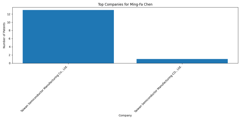
* Taiwan Semiconductor Manufacturing Company, Ltd.: | * Taiwan Semiconductor Manufacturing Company, Ltd.: 11 patents | ||
=== Collaborators === | === Collaborators === | ||
* [[:Category:Hsien-Wei Chen|Hsien-Wei Chen]][[Category:Hsien-Wei Chen]] ( | * [[:Category:Hsien-Wei Chen|Hsien-Wei Chen]][[Category:Hsien-Wei Chen]] (8 collaborations) | ||
* [[:Category:Jie Chen|Jie Chen]][[Category:Jie Chen]] ( | * [[:Category:Jie Chen|Jie Chen]][[Category:Jie Chen]] (5 collaborations) | ||
* [[:Category:Sung-Feng Yeh|Sung-Feng Yeh]][[Category:Sung-Feng Yeh]] (2 collaborations) | * [[:Category:Sung-Feng Yeh|Sung-Feng Yeh]][[Category:Sung-Feng Yeh]] (3 collaborations) | ||
* [[:Category:Ching-Jung Yang|Ching-Jung Yang]][[Category:Ching-Jung Yang]] (2 collaborations) | |||
* [[:Category:Ying-Ju Chen|Ying-Ju Chen]][[Category:Ying-Ju Chen]] (2 collaborations) | |||
* [[:Category:Tzuan-Horng Liu|Tzuan-Horng Liu]][[Category:Tzuan-Horng Liu]] (2 collaborations) | * [[:Category:Tzuan-Horng Liu|Tzuan-Horng Liu]][[Category:Tzuan-Horng Liu]] (2 collaborations) | ||
* [[:Category:Chao-Wen Shih|Chao-Wen Shih]][[Category:Chao-Wen Shih]] (2 collaborations) | * [[:Category:Chao-Wen Shih|Chao-Wen Shih]][[Category:Chao-Wen Shih]] (2 collaborations) | ||
* [[:Category:Sheng-An Kuo|Sheng-An Kuo]][[Category:Sheng-An Kuo]] (1 collaborations) | * [[:Category:Sheng-An Kuo|Sheng-An Kuo]][[Category:Sheng-An Kuo]] (1 collaborations) | ||
* [[:Category:Jen-Li Hu|Jen-Li Hu]][[Category:Jen-Li Hu]] (1 collaborations) | * [[:Category:Jen-Li Hu|Jen-Li Hu]][[Category:Jen-Li Hu]] (1 collaborations) | ||
* [[:Category:Jian-Wei Hong|Jian-Wei Hong]][[Category:Jian-Wei Hong]] (1 collaborations) | * [[:Category:Jian-Wei Hong|Jian-Wei Hong]][[Category:Jian-Wei Hong]] (1 collaborations) | ||
Latest revision as of 08:39, 2 May 2025
Ming-Fa Chen
Executive Summary
Ming-Fa Chen is an inventor who has filed 11 patents. Their primary areas of innovation include SEMICONDUCTOR DEVICES NOT COVERED BY CLASS (6 patents), SEMICONDUCTOR DEVICES NOT COVERED BY CLASS (5 patents), {Multistep manufacturing processes of assemblies consisting of devices, each device being of a type provided for in group (4 patents), and they have worked with companies such as Taiwan Semiconductor Manufacturing Company, Ltd. (11 patents). Their most frequent collaborators include (8 collaborations), (5 collaborations), (3 collaborations).
Patent Filing Activity
Technology Areas
List of Technology Areas
- H01L25/0657 (SEMICONDUCTOR DEVICES NOT COVERED BY CLASS): 6 patents
- H01L24/05 (SEMICONDUCTOR DEVICES NOT COVERED BY CLASS): 5 patents
- H01L25/50 ({Multistep manufacturing processes of assemblies consisting of devices, each device being of a type provided for in group): 4 patents
- H01L21/76877 ({Thin films associated with contacts of capacitors}): 3 patents
- H01L2224/08146 (SEMICONDUCTOR DEVICES NOT COVERED BY CLASS): 3 patents
- H01L24/08 (SEMICONDUCTOR DEVICES NOT COVERED BY CLASS): 3 patents
- H01L2225/06586 (SEMICONDUCTOR DEVICES NOT COVERED BY CLASS): 3 patents
- H01L21/76807 (Applying interconnections to be used for carrying current between separate components within a device {comprising conductors and dielectrics}): 2 patents
- H01L2224/02372 (SEMICONDUCTOR DEVICES NOT COVERED BY CLASS): 2 patents
- H01L21/78 (with subsequent division of the substrate into plural individual devices (cutting to change the surface-physical characteristics or shape of semiconductor bodies): 2 patents
- H01L21/561 (SEMICONDUCTOR DEVICES NOT COVERED BY CLASS): 2 patents
- H01L23/528 ({Geometry or} layout of the interconnection structure {(): 2 patents
- H01L24/06 ({of a plurality of bonding areas}): 2 patents
- H01L24/19 (SEMICONDUCTOR DEVICES NOT COVERED BY CLASS): 2 patents
- H01L23/5226 (SEMICONDUCTOR DEVICES NOT COVERED BY CLASS): 2 patents
- H01L24/03 (SEMICONDUCTOR DEVICES NOT COVERED BY CLASS): 2 patents
- H01L21/56 (SEMICONDUCTOR DEVICES NOT COVERED BY CLASS): 2 patents
- H01L2225/06548 (SEMICONDUCTOR DEVICES NOT COVERED BY CLASS): 2 patents
- H01L24/80 ({Methods for connecting semiconductor or other solid state bodies using means for bonding being attached to, or being formed on, the surface to be connected}): 2 patents
- H01L2224/80895 (SEMICONDUCTOR DEVICES NOT COVERED BY CLASS): 2 patents
- H01L2224/80896 (SEMICONDUCTOR DEVICES NOT COVERED BY CLASS): 2 patents
- H01L2225/06524 (SEMICONDUCTOR DEVICES NOT COVERED BY CLASS): 2 patents
- H01L2225/06541 (SEMICONDUCTOR DEVICES NOT COVERED BY CLASS): 2 patents
- H01L2224/02371 (SEMICONDUCTOR DEVICES NOT COVERED BY CLASS): 2 patents
- H01L27/0688 (SEMICONDUCTOR DEVICES NOT COVERED BY CLASS): 1 patents
- H01L23/5384 ({Conductive vias through the substrate with or without pins, e.g. buried coaxial conductors (): 1 patents
- H01L23/3114 (SEMICONDUCTOR DEVICES NOT COVERED BY CLASS): 1 patents
- H01L23/49816 (Leads, {i.e. metallisations or lead-frames} on insulating substrates, {e.g. chip carriers (shape of the substrate): 1 patents
- H01L23/5389 (the interconnection structure between a plurality of semiconductor chips being formed on, or in, insulating substrates ({): 1 patents
- H01L24/16 (SEMICONDUCTOR DEVICES NOT COVERED BY CLASS): 1 patents
- H01L2224/05008 (SEMICONDUCTOR DEVICES NOT COVERED BY CLASS): 1 patents
- H01L2224/05022 (SEMICONDUCTOR DEVICES NOT COVERED BY CLASS): 1 patents
- H01L2224/05099 (SEMICONDUCTOR DEVICES NOT COVERED BY CLASS): 1 patents
- H01L2224/12105 (SEMICONDUCTOR DEVICES NOT COVERED BY CLASS): 1 patents
- H01L2224/16145 (SEMICONDUCTOR DEVICES NOT COVERED BY CLASS): 1 patents
- H01L2924/181 (SEMICONDUCTOR DEVICES NOT COVERED BY CLASS): 1 patents
- H01L23/49503 (Lead-frames {or other flat leads (): 1 patents
- H01L21/76898 ({formed through a semiconductor substrate}): 1 patents
- H01L23/49827 ({Via connections through the substrates, e.g. pins going through the substrate, coaxial cables (): 1 patents
- H01L21/4846 (Manufacture or treatment of parts, e.g. containers, prior to assembly of the devices, using processes not provided for in a single one of the subgroups): 1 patents
- H01L24/13 (SEMICONDUCTOR DEVICES NOT COVERED BY CLASS): 1 patents
- H01L24/14 ({of a plurality of bump connectors}): 1 patents
- H01L24/81 (SEMICONDUCTOR DEVICES NOT COVERED BY CLASS): 1 patents
- H01L23/5222 ({Capacitive arrangements or effects of, or between wiring layers (other capacitive arrangements): 1 patents
- H01L23/645 ({Inductive arrangements (): 1 patents
- H01L2924/1205 (SEMICONDUCTOR DEVICES NOT COVERED BY CLASS): 1 patents
- H01L2924/1206 (SEMICONDUCTOR DEVICES NOT COVERED BY CLASS): 1 patents
- H01L23/3128 (SEMICONDUCTOR DEVICES NOT COVERED BY CLASS): 1 patents
- H01L23/481 (Arrangements for conducting electric current to or from the solid state body in operation, e.g. leads, terminal arrangements {; Selection of materials therefor}): 1 patents
- H01L24/24 (SEMICONDUCTOR DEVICES NOT COVERED BY CLASS): 1 patents
- H01L24/89 (SEMICONDUCTOR DEVICES NOT COVERED BY CLASS): 1 patents
- H10D1/692 (No explanation available): 1 patents
- H01L2224/0557 (SEMICONDUCTOR DEVICES NOT COVERED BY CLASS): 1 patents
- H01L2224/24145 (SEMICONDUCTOR DEVICES NOT COVERED BY CLASS): 1 patents
- H01L2224/80001 (SEMICONDUCTOR DEVICES NOT COVERED BY CLASS): 1 patents
- H01L2225/06568 (SEMICONDUCTOR DEVICES NOT COVERED BY CLASS): 1 patents
- H01L2924/19041 (SEMICONDUCTOR DEVICES NOT COVERED BY CLASS): 1 patents
- H01L33/52 (Encapsulations): 1 patents
- G02B6/12004 (of the integrated circuit kind (electric integrated circuits): 1 patents
- G02B6/4206 (Coupling light guides with opto-electronic elements): 1 patents
- H01L25/167 (the devices being of types provided for in two or more different main groups of groups): 1 patents
- H01L31/0203 (Containers; Encapsulations {, e.g. encapsulation of photodiodes} (for photovoltaic devices): 1 patents
- H01L31/02325 (Optical elements or arrangements associated with the device (): 1 patents
- H01L31/18 (Processes or apparatus specially adapted for the manufacture or treatment of these devices or of parts thereof): 1 patents
- H01L33/58 (Optical field-shaping elements): 1 patents
- H01L33/62 (Arrangements for conducting electric current to or from the semiconductor body, e.g. lead-frames, wire-bonds or solder balls): 1 patents
- H01L2933/005 (SEMICONDUCTOR DEVICES NOT COVERED BY CLASS): 1 patents
- H01L2933/0058 (SEMICONDUCTOR DEVICES NOT COVERED BY CLASS): 1 patents
- H01L21/6835 ({using temporarily an auxiliary support}): 1 patents
- H01L23/60 (Protection against electrostatic charges or discharges, e.g. Faraday shields): 1 patents
- H01L2221/68331 (SEMICONDUCTOR DEVICES NOT COVERED BY CLASS): 1 patents
- H01L2224/80006 (SEMICONDUCTOR DEVICES NOT COVERED BY CLASS): 1 patents
- H01L2224/8013 (SEMICONDUCTOR DEVICES NOT COVERED BY CLASS): 1 patents
- H01L2225/06527 (SEMICONDUCTOR DEVICES NOT COVERED BY CLASS): 1 patents
- H01L2225/06593 (SEMICONDUCTOR DEVICES NOT COVERED BY CLASS): 1 patents
- H01L2924/30205 (SEMICONDUCTOR DEVICES NOT COVERED BY CLASS): 1 patents
- H01L23/3121 (SEMICONDUCTOR DEVICES NOT COVERED BY CLASS): 1 patents
- H01L24/29 (SEMICONDUCTOR DEVICES NOT COVERED BY CLASS): 1 patents
- H01L2924/3511 (SEMICONDUCTOR DEVICES NOT COVERED BY CLASS): 1 patents
- H01L21/565 (SEMICONDUCTOR DEVICES NOT COVERED BY CLASS): 1 patents
- H01L2224/06519 (SEMICONDUCTOR DEVICES NOT COVERED BY CLASS): 1 patents
- H01L2224/08145 (SEMICONDUCTOR DEVICES NOT COVERED BY CLASS): 1 patents
- H01L2225/06589 (SEMICONDUCTOR DEVICES NOT COVERED BY CLASS): 1 patents
- H10D88/00 (No explanation available): 1 patents
- H01L21/76816 ({Aspects relating to the layout of the pattern or to the size of vias or trenches (layout of the interconnections per se): 1 patents
- H01L24/09 (SEMICONDUCTOR DEVICES NOT COVERED BY CLASS): 1 patents
- H01L24/33 (SEMICONDUCTOR DEVICES NOT COVERED BY CLASS): 1 patents
- H01L2224/02379 (SEMICONDUCTOR DEVICES NOT COVERED BY CLASS): 1 patents
Companies
List of Companies
- Taiwan Semiconductor Manufacturing Company, Ltd.: 11 patents
Collaborators
- Hsien-Wei Chen (8 collaborations)
- Jie Chen (5 collaborations)
- Sung-Feng Yeh (3 collaborations)
- Ching-Jung Yang (2 collaborations)
- Ying-Ju Chen (2 collaborations)
- Tzuan-Horng Liu (2 collaborations)
- Chao-Wen Shih (2 collaborations)
- Sheng-An Kuo (1 collaborations)
- Jen-Li Hu (1 collaborations)
- Jian-Wei Hong (1 collaborations)
Subcategories
This category has the following 2 subcategories, out of 2 total.
H
M
(Ad) Transform your business with AI in minutes, not months
Trusted by 1,000+ companies worldwide


