Category:Tomotaka MORISHITA
Appearance
Tomotaka MORISHITA
Executive Summary
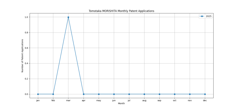
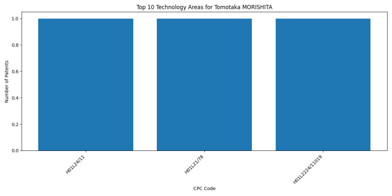
Tomotaka MORISHITA is an inventor who has filed 1 patents. Their primary areas of innovation include {Manufacturing methods (for bumps on insulating substrates (1 patents), with subsequent division of the substrate into plural individual devices (cutting to change the surface-physical characteristics or shape of semiconductor bodies (1 patents), SEMICONDUCTOR DEVICES NOT COVERED BY CLASS (1 patents), and they have worked with companies such as LINTEC CORPORATION (1 patents). Their most frequent collaborators include (1 collaborations).
Patent Filing Activity
Technology Areas
List of Technology Areas
- H01L24/11 ({Manufacturing methods (for bumps on insulating substrates): 1 patents
- H01L21/78 (with subsequent division of the substrate into plural individual devices (cutting to change the surface-physical characteristics or shape of semiconductor bodies): 1 patents
- H01L2224/11019 (SEMICONDUCTOR DEVICES NOT COVERED BY CLASS): 1 patents
Companies
Error creating thumbnail: File missing
List of Companies
- LINTEC CORPORATION: 1 patents
Collaborators
- Keisuke SHINOMIYA (1 collaborations)
Subcategories
This category has the following 2 subcategories, out of 2 total.

