Category:Oseob Jeon
Appearance
Oseob Jeon
Executive Summary
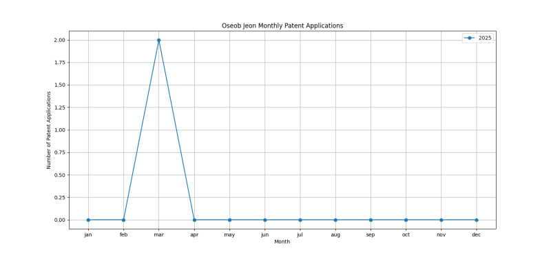
Oseob Jeon is an inventor who has filed 2 patents. Their primary areas of innovation include {Additional leads joined to the metallisation on the insulating substrate, e.g. pins, bumps, wires, flat leads ( (2 patents), SEMICONDUCTOR DEVICES NOT COVERED BY CLASS (1 patents), Cooling facilitated by shape of device {( (1 patents), and they have worked with companies such as Navitas Semiconductor Limited (2 patents). Their most frequent collaborators include .
Patent Filing Activity
Technology Areas
List of Technology Areas
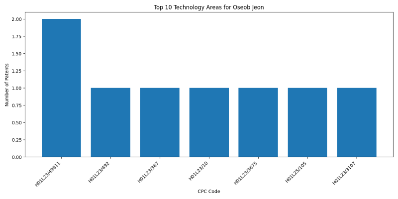
- H01L23/49811 ({Additional leads joined to the metallisation on the insulating substrate, e.g. pins, bumps, wires, flat leads (): 2 patents
- H01L23/492 (SEMICONDUCTOR DEVICES NOT COVERED BY CLASS): 1 patents
- H01L23/367 (Cooling facilitated by shape of device {(): 1 patents
- H01L23/10 (SEMICONDUCTOR DEVICES NOT COVERED BY CLASS): 1 patents
- H01L23/3675 (Cooling facilitated by shape of device {(): 1 patents
- H01L25/105 (SEMICONDUCTOR DEVICES NOT COVERED BY CLASS): 1 patents
- H01L23/3107 (SEMICONDUCTOR DEVICES NOT COVERED BY CLASS): 1 patents
Companies
List of Companies
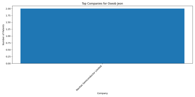
- Navitas Semiconductor Limited: 2 patents


