Category:Kazuya HIRATA
Kazuya HIRATA
Executive Summary
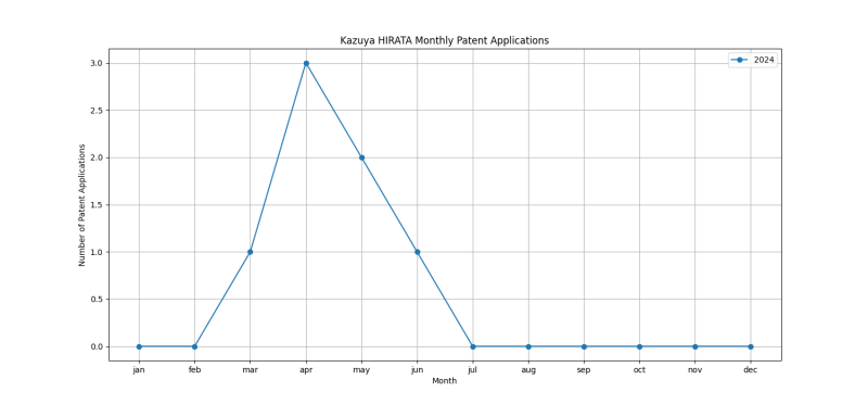
Kazuya HIRATA is an inventor who has filed 3 patents. Their primary areas of innovation include SOLDERING OR UNSOLDERING; WELDING; CLADDING OR PLATING BY SOLDERING OR WELDING; CUTTING BY APPLYING HEAT LOCALLY, e.g. FLAME CUTTING; WORKING BY LASER BEAM (making metal-coated products by extruding metal (2 patents), Working by laser beam, e.g. welding, cutting or boring (2 patents), SOLDERING OR UNSOLDERING; WELDING; CLADDING OR PLATING BY SOLDERING OR WELDING; CUTTING BY APPLYING HEAT LOCALLY, e.g. FLAME CUTTING; WORKING BY LASER BEAM (making metal-coated products by extruding metal (2 patents), and they have worked with companies such as DISCO CORPORATION (3 patents). Their most frequent collaborators include (1 collaborations), (1 collaborations), (1 collaborations).
Patent Filing Activity
Technology Areas
List of Technology Areas
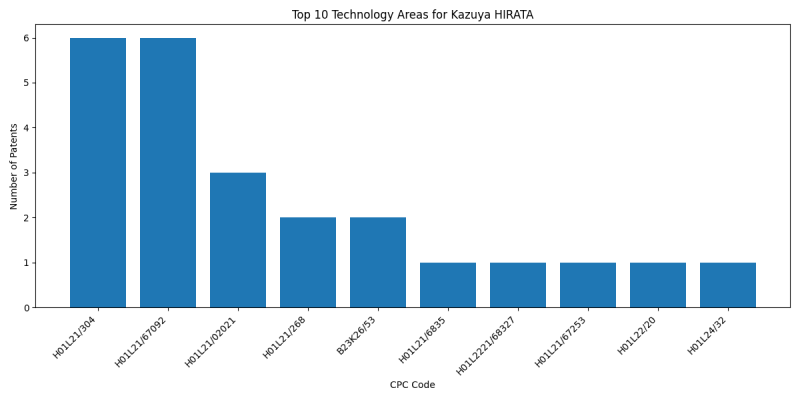
- B23K26/53 (SOLDERING OR UNSOLDERING; WELDING; CLADDING OR PLATING BY SOLDERING OR WELDING; CUTTING BY APPLYING HEAT LOCALLY, e.g. FLAME CUTTING; WORKING BY LASER BEAM (making metal-coated products by extruding metal): 2 patents
- B23K26/0093 (Working by laser beam, e.g. welding, cutting or boring): 2 patents
- B23K2101/40 (SOLDERING OR UNSOLDERING; WELDING; CLADDING OR PLATING BY SOLDERING OR WELDING; CUTTING BY APPLYING HEAT LOCALLY, e.g. FLAME CUTTING; WORKING BY LASER BEAM (making metal-coated products by extruding metal): 2 patents
- B23K26/066 (by using masks): 1 patents
- B23K26/0622 (SOLDERING OR UNSOLDERING; WELDING; CLADDING OR PLATING BY SOLDERING OR WELDING; CUTTING BY APPLYING HEAT LOCALLY, e.g. FLAME CUTTING; WORKING BY LASER BEAM (making metal-coated products by extruding metal): 1 patents
- H01L23/544 (Marks applied to semiconductor devices {or parts}, e.g. registration marks, {alignment structures, wafer maps (test patterns for characterising or monitoring manufacturing processes): 1 patents
- B23K26/364 (Removing material (): 1 patents
- H01L22/12 ({for structural parameters, e.g. thickness, line width, refractive index, temperature, warp, bond strength, defects, optical inspection, electrical measurement of structural dimensions, metallurgic measurement of diffusions (electrical measurement of diffusions): 1 patents
- H01L2223/54493 (SEMICONDUCTOR DEVICES NOT COVERED BY CLASS): 1 patents
- B28D5/047 (WORKING STONE OR STONE-LIKE MATERIALS): 1 patents
- B28D5/0082 (Fine working of gems, jewels, crystals, e.g. of semiconductor material; apparatus or devices therefor (working by grinding or polishing): 1 patents
Companies
List of Companies
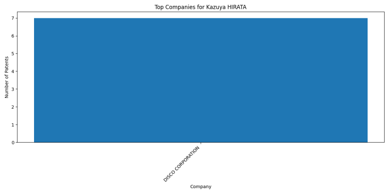
- DISCO CORPORATION: 3 patents
Collaborators
- Asahi NOMOTO (1 collaborations)
- Nobuki KAKIUCHI (1 collaborations)
- Tomoki YOSHINO (1 collaborations)
Subcategories
This category has the following 4 subcategories, out of 4 total.


