Category:Kazunori FUJI
Appearance
Kazunori FUJI
Executive Summary
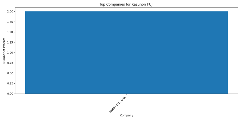
Kazunori FUJI is an inventor who has filed 2 patents. Their primary areas of innovation include Devices involving relative movement between laser beam and workpiece (1 patents), SOLDERING OR UNSOLDERING; WELDING; CLADDING OR PLATING BY SOLDERING OR WELDING; CUTTING BY APPLYING HEAT LOCALLY, e.g. FLAME CUTTING; WORKING BY LASER BEAM (making metal-coated products by extruding metal (1 patents), SEMICONDUCTOR DEVICES NOT COVERED BY CLASS (1 patents), and they have worked with companies such as ROHM CO., LTD. (2 patents). Their most frequent collaborators include (1 collaborations).
Patent Filing Activity
Technology Areas
List of Technology Areas
- B23K26/082 (Devices involving relative movement between laser beam and workpiece): 1 patents
- B23K26/21 (SOLDERING OR UNSOLDERING; WELDING; CLADDING OR PLATING BY SOLDERING OR WELDING; CUTTING BY APPLYING HEAT LOCALLY, e.g. FLAME CUTTING; WORKING BY LASER BEAM (making metal-coated products by extruding metal): 1 patents
- H01L24/03 (SEMICONDUCTOR DEVICES NOT COVERED BY CLASS): 1 patents
- H01L24/04 (SEMICONDUCTOR DEVICES NOT COVERED BY CLASS): 1 patents
- H01L2224/4847 (SEMICONDUCTOR DEVICES NOT COVERED BY CLASS): 1 patents
- H01L2224/73265 (SEMICONDUCTOR DEVICES NOT COVERED BY CLASS): 1 patents
- H01L21/7813 (with subsequent division of the substrate into plural individual devices (cutting to change the surface-physical characteristics or shape of semiconductor bodies): 1 patents
- B23K26/53 (SOLDERING OR UNSOLDERING; WELDING; CLADDING OR PLATING BY SOLDERING OR WELDING; CUTTING BY APPLYING HEAT LOCALLY, e.g. FLAME CUTTING; WORKING BY LASER BEAM (making metal-coated products by extruding metal): 1 patents
- H01L21/304 (Mechanical treatment, e.g. grinding, polishing, cutting {(): 1 patents
- H01L21/30625 ({With simultaneous mechanical treatment, e.g. mechanico-chemical polishing}): 1 patents
- H01L21/6835 ({using temporarily an auxiliary support}): 1 patents
- H01L23/544 (Marks applied to semiconductor devices {or parts}, e.g. registration marks, {alignment structures, wafer maps (test patterns for characterising or monitoring manufacturing processes): 1 patents
- H01L2221/68345 (SEMICONDUCTOR DEVICES NOT COVERED BY CLASS): 1 patents
- H01L2221/6835 (SEMICONDUCTOR DEVICES NOT COVERED BY CLASS): 1 patents
Companies
List of Companies
- ROHM CO., LTD.: 2 patents
Collaborators
- Masatoshi AKETA (1 collaborations)


