Category:Hung-Jui Kuo
Appearance
Hung-Jui Kuo
Executive Summary
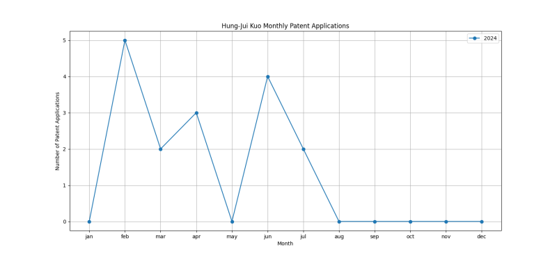
Hung-Jui Kuo is an inventor who has filed 12 patents. Their primary areas of innovation include {Multilayer substrates ( (6 patents), SEMICONDUCTOR DEVICES NOT COVERED BY CLASS (5 patents), SEMICONDUCTOR DEVICES NOT COVERED BY CLASS (5 patents), and they have worked with companies such as Taiwan Semiconductor Manufacturing Company, Ltd. (10 patents), Taiwan Semiconductor Manufacturing Company Limited (2 patents). Their most frequent collaborators include (6 collaborations), (4 collaborations), (3 collaborations).
Patent Filing Activity
Technology Areas
List of Technology Areas
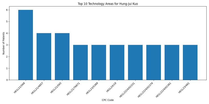
- H01L23/5383 ({Multilayer substrates (): 6 patents
- H01L21/568 (SEMICONDUCTOR DEVICES NOT COVERED BY CLASS): 5 patents
- H01L23/3128 (SEMICONDUCTOR DEVICES NOT COVERED BY CLASS): 5 patents
- H01L23/5389 (the interconnection structure between a plurality of semiconductor chips being formed on, or in, insulating substrates ({): 4 patents
- H01L21/4853 (Manufacture or treatment of parts, e.g. containers, prior to assembly of the devices, using processes not provided for in a single one of the subgroups): 4 patents
- H01L21/4857 (Manufacture or treatment of parts, e.g. containers, prior to assembly of the devices, using processes not provided for in a single one of the subgroups): 4 patents
- H01L21/565 (SEMICONDUCTOR DEVICES NOT COVERED BY CLASS): 4 patents
- H01L23/5386 (the interconnection structure between a plurality of semiconductor chips being formed on, or in, insulating substrates ({): 4 patents
- H01L24/19 (SEMICONDUCTOR DEVICES NOT COVERED BY CLASS): 4 patents
- H01L24/20 (SEMICONDUCTOR DEVICES NOT COVERED BY CLASS): 4 patents
- H01L2224/214 (SEMICONDUCTOR DEVICES NOT COVERED BY CLASS): 4 patents
- H01L23/544 (Marks applied to semiconductor devices {or parts}, e.g. registration marks, {alignment structures, wafer maps (test patterns for characterising or monitoring manufacturing processes): 3 patents
- H01L2223/54426 (SEMICONDUCTOR DEVICES NOT COVERED BY CLASS): 3 patents
- H01L25/105 (SEMICONDUCTOR DEVICES NOT COVERED BY CLASS): 3 patents
- H01L21/4864 (Manufacture or treatment of parts, e.g. containers, prior to assembly of the devices, using processes not provided for in a single one of the subgroups): 2 patents
- H01L21/6835 ({using temporarily an auxiliary support}): 2 patents
- H01L23/564 (SEMICONDUCTOR DEVICES NOT COVERED BY CLASS): 2 patents
- H01L2221/68372 (SEMICONDUCTOR DEVICES NOT COVERED BY CLASS): 2 patents
- H01L21/78 (with subsequent division of the substrate into plural individual devices (cutting to change the surface-physical characteristics or shape of semiconductor bodies): 2 patents
- H01L23/5384 ({Conductive vias through the substrate with or without pins, e.g. buried coaxial conductors (): 2 patents
- H01L24/32 (SEMICONDUCTOR DEVICES NOT COVERED BY CLASS): 2 patents
- H01L21/56 (SEMICONDUCTOR DEVICES NOT COVERED BY CLASS): 2 patents
- H01L23/31 (SEMICONDUCTOR DEVICES NOT COVERED BY CLASS): 2 patents
- H01L23/528 ({Geometry or} layout of the interconnection structure {(): 2 patents
- H01L23/481 (Arrangements for conducting electric current to or from the solid state body in operation, e.g. leads, terminal arrangements {; Selection of materials therefor}): 2 patents
- H01L23/49822 ({Multilayer substrates (multilayer metallisation on monolayer substrate): 2 patents
- H01L23/3121 (SEMICONDUCTOR DEVICES NOT COVERED BY CLASS): 1 patents
- H01L23/562 (SEMICONDUCTOR DEVICES NOT COVERED BY CLASS): 1 patents
- H01L23/585 ({comprising conductive layers or plates or strips or rods or rings (): 1 patents
- H01L21/68742 (using mechanical means, e.g. chucks, clamps or pinches {(using elecrostatic chucks): 1 patents
- G03F7/70708 (PHOTOMECHANICAL PRODUCTION OF TEXTURED OR PATTERNED SURFACES, e.g. FOR PRINTING, FOR PROCESSING OF SEMICONDUCTOR DEVICES; MATERIALS THEREFOR; ORIGINALS THEREFOR; APPARATUS SPECIALLY ADAPTED THEREFOR; (phototypographic composing devices): 1 patents
- H01L21/561 (SEMICONDUCTOR DEVICES NOT COVERED BY CLASS): 1 patents
- H01L23/5385 (the interconnection structure between a plurality of semiconductor chips being formed on, or in, insulating substrates ({): 1 patents
- H01L24/16 (SEMICONDUCTOR DEVICES NOT COVERED BY CLASS): 1 patents
- H01L24/73 (SEMICONDUCTOR DEVICES NOT COVERED BY CLASS): 1 patents
- H01L2224/16235 (SEMICONDUCTOR DEVICES NOT COVERED BY CLASS): 1 patents
- H01L2224/32225 (SEMICONDUCTOR DEVICES NOT COVERED BY CLASS): 1 patents
- H01L2224/73204 (SEMICONDUCTOR DEVICES NOT COVERED BY CLASS): 1 patents
- H01L2924/364 (SEMICONDUCTOR DEVICES NOT COVERED BY CLASS): 1 patents
- G03F7/426 ({containing organic halogen compounds; containing organic sulfonic acids or salts thereof; containing sulfoxides}): 1 patents
- H01L23/5226 (SEMICONDUCTOR DEVICES NOT COVERED BY CLASS): 1 patents
- H01L21/76802 (Applying interconnections to be used for carrying current between separate components within a device {comprising conductors and dielectrics}): 1 patents
- H01L24/03 (SEMICONDUCTOR DEVICES NOT COVERED BY CLASS): 1 patents
- H01L24/05 (SEMICONDUCTOR DEVICES NOT COVERED BY CLASS): 1 patents
- H01L2224/0346 (SEMICONDUCTOR DEVICES NOT COVERED BY CLASS): 1 patents
- H01L2224/05546 (SEMICONDUCTOR DEVICES NOT COVERED BY CLASS): 1 patents
- H01L21/76898 ({formed through a semiconductor substrate}): 1 patents
- H01L21/76804 ({by forming tapered via holes}): 1 patents
- H01L21/76846 ({Layer combinations}): 1 patents
- H01L21/76871 ({Layers specifically deposited to enhance or enable the nucleation of further layers, i.e. seed layers}): 1 patents
- H01L23/49816 (Leads, {i.e. metallisations or lead-frames} on insulating substrates, {e.g. chip carriers (shape of the substrate): 1 patents
- H01L23/49838 (Leads, {i.e. metallisations or lead-frames} on insulating substrates, {e.g. chip carriers (shape of the substrate): 1 patents
- H01L2225/1041 (SEMICONDUCTOR DEVICES NOT COVERED BY CLASS): 1 patents
- H01L24/14 ({of a plurality of bump connectors}): 1 patents
- H01L25/50 ({Multistep manufacturing processes of assemblies consisting of devices, each device being of a type provided for in group): 1 patents
- H01L24/82 ({by forming build-up interconnects at chip-level, e.g. for high density interconnects [HDI] (interconnection structure between a plurality of semiconductor chips): 1 patents
- H01L24/80 ({Methods for connecting semiconductor or other solid state bodies using means for bonding being attached to, or being formed on, the surface to be connected}): 1 patents
- H01L24/95 (SEMICONDUCTOR DEVICES NOT COVERED BY CLASS): 1 patents
- H01L25/0657 (SEMICONDUCTOR DEVICES NOT COVERED BY CLASS): 1 patents
- H10D88/00 (No explanation available): 1 patents
- H01L2224/80896 (SEMICONDUCTOR DEVICES NOT COVERED BY CLASS): 1 patents
- H01L24/13 (SEMICONDUCTOR DEVICES NOT COVERED BY CLASS): 1 patents
- H01L25/0655 (SEMICONDUCTOR DEVICES NOT COVERED BY CLASS): 1 patents
- H01L2224/13007 (SEMICONDUCTOR DEVICES NOT COVERED BY CLASS): 1 patents
- H01L2224/32146 (SEMICONDUCTOR DEVICES NOT COVERED BY CLASS): 1 patents
- H01L2224/32235 (SEMICONDUCTOR DEVICES NOT COVERED BY CLASS): 1 patents
- H01L2924/15311 (SEMICONDUCTOR DEVICES NOT COVERED BY CLASS): 1 patents
- H01L2924/182 (SEMICONDUCTOR DEVICES NOT COVERED BY CLASS): 1 patents
Companies
List of Companies
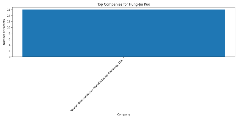
- Taiwan Semiconductor Manufacturing Company, Ltd.: 10 patents
- Taiwan Semiconductor Manufacturing Company Limited: 2 patents
Collaborators
- Yu-Hsiang Hu (6 collaborations)
- Jhih-Yu Wang (4 collaborations)
- Po-Han Wang (3 collaborations)
- Hui-Jung Tsai (3 collaborations)
- Yung-Chi Chu (2 collaborations)
- Sih-Hao Liao (2 collaborations)
- Ming-Che Ho (2 collaborations)
- Tai-Min Chang (2 collaborations)
- Meng-Che Tu (2 collaborations)
- Chia-Wei Wang (2 collaborations)
- Wei-Yu Tsai (1 collaborations)
- Ming-Tan Lee (1 collaborations)
- Ching-Wen Chen (1 collaborations)
- Wei-Chung Chang (1 collaborations)
- Yu-Tzu Chang (1 collaborations)
Categories:
- Yu-Hsiang Hu
- Jhih-Yu Wang
- Po-Han Wang
- Hui-Jung Tsai
- Yung-Chi Chu
- Sih-Hao Liao
- Ming-Che Ho
- Tai-Min Chang
- Meng-Che Tu
- Chia-Wei Wang
- Wei-Yu Tsai
- Ming-Tan Lee
- Ching-Wen Chen
- Wei-Chung Chang
- Yu-Tzu Chang
- Hung-Jui Kuo
- Inventors
- Inventors filing patents with Taiwan Semiconductor Manufacturing Company, Ltd.
- Inventors filing patents with Taiwan Semiconductor Manufacturing Company Limited


