Category:Hitoshi TAKANE
Appearance
Hitoshi TAKANE
Executive Summary
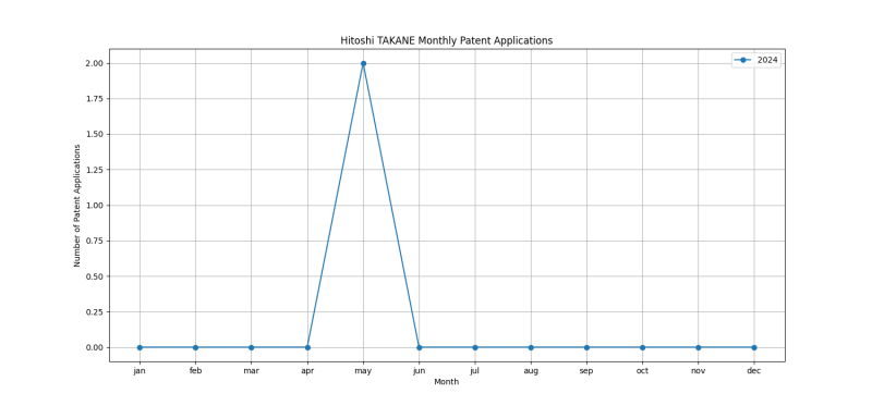
Hitoshi TAKANE is an inventor who has filed 2 patents. Their primary areas of innovation include SEMICONDUCTOR DEVICES NOT COVERED BY CLASS (2 patents), SEMICONDUCTOR DEVICES NOT COVERED BY CLASS (1 patents), SEMICONDUCTOR DEVICES NOT COVERED BY CLASS (1 patents), and they have worked with companies such as FLOSFIA INC. (2 patents). Their most frequent collaborators include (2 collaborations), (2 collaborations).
Patent Filing Activity
Technology Areas
List of Technology Areas
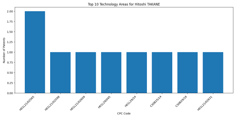
- H01L21/02565 (SEMICONDUCTOR DEVICES NOT COVERED BY CLASS): 2 patents
- H01L21/02598 (SEMICONDUCTOR DEVICES NOT COVERED BY CLASS): 1 patents
- H01L21/02609 (SEMICONDUCTOR DEVICES NOT COVERED BY CLASS): 1 patents
- H01L29/045 (SEMICONDUCTOR DEVICES NOT COVERED BY CLASS): 1 patents
- H01L29/24 (SEMICONDUCTOR DEVICES NOT COVERED BY CLASS): 1 patents
- C30B25/14 (SINGLE-CRYSTAL GROWTH (by using ultra-high pressure, e.g. for the formation of diamonds,): 1 patents
- C30B29/16 (SINGLE-CRYSTAL GROWTH (by using ultra-high pressure, e.g. for the formation of diamonds,): 1 patents
- H01L21/02631 (SEMICONDUCTOR DEVICES NOT COVERED BY CLASS): 1 patents
Companies
List of Companies
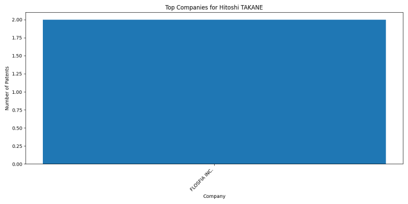
- FLOSFIA INC.: 2 patents
Collaborators
- Kentaro KANEKO (2 collaborations)
- Toshimi HITORA (2 collaborations)
Subcategories
This category has the following 2 subcategories, out of 2 total.


