Category:Chun-Wei CHIANG
Appearance
Chun-Wei CHIANG
Executive Summary
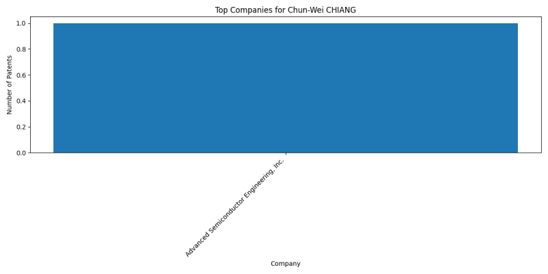
Chun-Wei CHIANG is an inventor who has filed 1 patents. Their primary areas of innovation include {Geometry or} layout of the interconnection structure {( (1 patents), {Filling up the space between adjacent conductive structures; Gap-filling properties of dielectrics} (1 patents), {Layers specifically deposited to enhance or enable the nucleation of further layers, i.e. seed layers} (1 patents), and they have worked with companies such as Advanced Semiconductor Engineering, Inc. (1 patents). Their most frequent collaborators include (1 collaborations), (1 collaborations), (1 collaborations).
Patent Filing Activity
Technology Areas
List of Technology Areas
- H01L23/5283 ({Geometry or} layout of the interconnection structure {(): 1 patents
- H01L21/76837 ({Filling up the space between adjacent conductive structures; Gap-filling properties of dielectrics}): 1 patents
- H01L21/76871 ({Layers specifically deposited to enhance or enable the nucleation of further layers, i.e. seed layers}): 1 patents
- H01L23/49811 ({Additional leads joined to the metallisation on the insulating substrate, e.g. pins, bumps, wires, flat leads (): 1 patents
- H01L23/5226 (SEMICONDUCTOR DEVICES NOT COVERED BY CLASS): 1 patents
Companies
List of Companies
- Advanced Semiconductor Engineering, Inc.: 1 patents
Collaborators
- Yung-Sheng LIN (1 collaborations)
- I-Ting LIN (1 collaborations)
- Ping-Hung HSIEH (1 collaborations)
- Chih-Yuan HSU (1 collaborations)


