Category:Biqi LI
Appearance
Biqi LI
Executive Summary
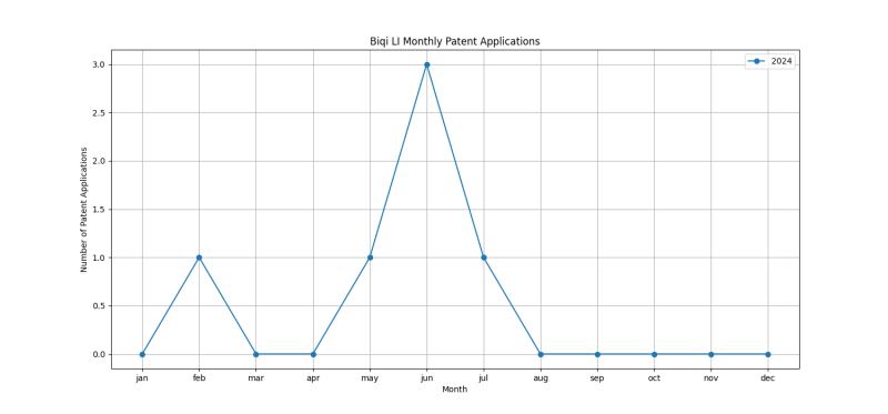
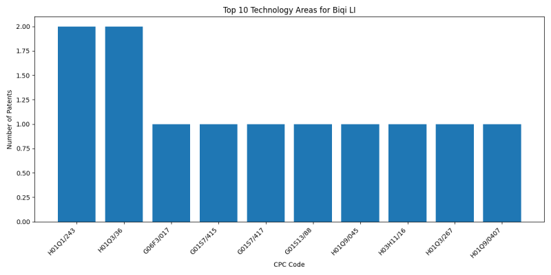
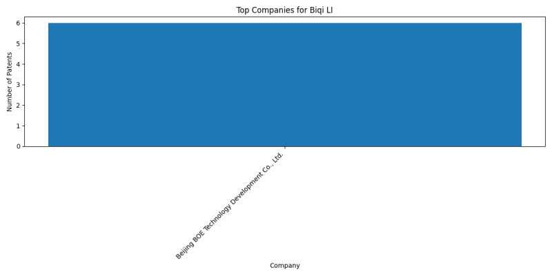
Biqi LI is an inventor who has filed 6 patents. Their primary areas of innovation include based on liquid crystals, e.g. single liquid crystal display cells (3 patents), SEMICONDUCTOR DEVICES NOT COVERED BY CLASS (2 patents), Leads, {i.e. metallisations or lead-frames} on insulating substrates, {e.g. chip carriers (shape of the substrate (2 patents), and they have worked with companies such as Beijing BOE Optoelectronics Technology Co., Ltd. (4 patents), BEIJING BOE OPTOELECTRONICS TECHNOLOGY CO., LTD. (2 patents). Their most frequent collaborators include (3 collaborations), (3 collaborations), (3 collaborations).
Patent Filing Activity
Technology Areas
List of Technology Areas
- G02F1/136286 (based on liquid crystals, e.g. single liquid crystal display cells): 3 patents
- H01L23/15 (SEMICONDUCTOR DEVICES NOT COVERED BY CLASS): 2 patents
- H01L23/49838 (Leads, {i.e. metallisations or lead-frames} on insulating substrates, {e.g. chip carriers (shape of the substrate): 2 patents
- H05K2201/10015 (PRINTED CIRCUITS; CASINGS OR CONSTRUCTIONAL DETAILS OF ELECTRIC APPARATUS; MANUFACTURE OF ASSEMBLAGES OF ELECTRICAL COMPONENTS): 2 patents
- H05K2201/1003 (PRINTED CIRCUITS; CASINGS OR CONSTRUCTIONAL DETAILS OF ELECTRIC APPARATUS; MANUFACTURE OF ASSEMBLAGES OF ELECTRICAL COMPONENTS): 2 patents
- G02F1/136209 (based on liquid crystals, e.g. single liquid crystal display cells): 2 patents
- G02F1/1368 (based on liquid crystals, e.g. single liquid crystal display cells): 2 patents
- H01L23/49833 (Leads, {i.e. metallisations or lead-frames} on insulating substrates, {e.g. chip carriers (shape of the substrate): 1 patents
- H01L21/4857 (Manufacture or treatment of parts, e.g. containers, prior to assembly of the devices, using processes not provided for in a single one of the subgroups): 1 patents
- H01L23/49816 (Leads, {i.e. metallisations or lead-frames} on insulating substrates, {e.g. chip carriers (shape of the substrate): 1 patents
- H01L23/49822 ({Multilayer substrates (multilayer metallisation on monolayer substrate): 1 patents
- H01L24/16 (SEMICONDUCTOR DEVICES NOT COVERED BY CLASS): 1 patents
- H01L2224/16227 (SEMICONDUCTOR DEVICES NOT COVERED BY CLASS): 1 patents
- H01L2224/16237 (SEMICONDUCTOR DEVICES NOT COVERED BY CLASS): 1 patents
- H01L2924/1511 (SEMICONDUCTOR DEVICES NOT COVERED BY CLASS): 1 patents
- H05K1/181 (Printed circuits structurally associated with non-printed electric components ({): 1 patents
- H05K2201/10378 (PRINTED CIRCUITS; CASINGS OR CONSTRUCTIONAL DETAILS OF ELECTRIC APPARATUS; MANUFACTURE OF ASSEMBLAGES OF ELECTRICAL COMPONENTS): 1 patents
- H05K1/182 (Printed circuits structurally associated with non-printed electric components ({): 1 patents
- H04B5/43 (TRANSMISSION): 1 patents
- G02F1/136222 (based on liquid crystals, e.g. single liquid crystal display cells): 1 patents
- G06F3/046 (by electromagnetic means): 1 patents
- H04B5/26 (TRANSMISSION): 1 patents
- G02F1/133357 (Constructional arrangements; Operation of liquid crystal cells; Circuit arrangements (arrangements or circuits for control of liquid crystal elements in a matrix, not structurally associated with these elements): 1 patents
- G02F1/13338 ({Input devices, e.g. touch panels}): 1 patents
- G02F1/134363 (based on liquid crystals, e.g. single liquid crystal display cells): 1 patents
- G02F1/136227 (based on liquid crystals, e.g. single liquid crystal display cells): 1 patents
- G06F3/0412 ({Digitisers structurally integrated in a display}): 1 patents
- G06F3/04164 ({Connections between sensors and controllers, e.g. routing lines between electrodes and connection pads}): 1 patents
- H01Q1/22 (by structural association with other equipment or articles): 1 patents
- G02F1/133512 (Structural association of cells with optical devices, e.g. polarisers or reflectors): 1 patents
- G06F3/044 (by capacitive means): 1 patents
- H01L23/645 ({Inductive arrangements (): 1 patents
- H01L21/486 (Manufacture or treatment of parts, e.g. containers, prior to assembly of the devices, using processes not provided for in a single one of the subgroups): 1 patents
- H01L23/49827 ({Via connections through the substrates, e.g. pins going through the substrate, coaxial cables (): 1 patents
- H05K1/0306 (Use of materials for the substrate): 1 patents
- H05K1/115 (PRINTED CIRCUITS; CASINGS OR CONSTRUCTIONAL DETAILS OF ELECTRIC APPARATUS; MANUFACTURE OF ASSEMBLAGES OF ELECTRICAL COMPONENTS): 1 patents
- H05K3/4038 (PRINTED CIRCUITS; CASINGS OR CONSTRUCTIONAL DETAILS OF ELECTRIC APPARATUS; MANUFACTURE OF ASSEMBLAGES OF ELECTRICAL COMPONENTS): 1 patents
- H05K2201/09509 (PRINTED CIRCUITS; CASINGS OR CONSTRUCTIONAL DETAILS OF ELECTRIC APPARATUS; MANUFACTURE OF ASSEMBLAGES OF ELECTRICAL COMPONENTS): 1 patents
Companies
List of Companies
- Beijing BOE Optoelectronics Technology Co., Ltd.: 4 patents
- BEIJING BOE OPTOELECTRONICS TECHNOLOGY CO., LTD.: 2 patents
Collaborators
- Yifan WU (3 collaborations)
- Yue LI (3 collaborations)
- Yuelei XIAO (3 collaborations)
- Yulin FENG (3 collaborations)
- Qichang AN (3 collaborations)
- Yu ZHAO (3 collaborations)
- Jian WANG (3 collaborations)
- Xiaojuan WU (3 collaborations)
- Dawei FENG (3 collaborations)
- Xiaodong LI (2 collaborations)
- Jingshu ZHANG (2 collaborations)
- Kidong HAN (2 collaborations)
- Huiying LI (2 collaborations)
- Zhiqiang YU (2 collaborations)
- Chunnan FENG (2 collaborations)
- Yao BI (2 collaborations)
- Jinshuai DUAN (2 collaborations)
- Jiaxing WANG (2 collaborations)
- Feng LIU (2 collaborations)
- Cuiyu CHEN (2 collaborations)
- Yingwei LIU (1 collaborations)
- Zijian WANG (1 collaborations)
- Rui MA (1 collaborations)
- Quanyue LI (1 collaborations)
- Song CHEN (1 collaborations)
- Qianyu GUO (1 collaborations)
- Xian WANG (1 collaborations)
- Yong ZHANG (1 collaborations)
- Lei SHI (1 collaborations)
- Yang GE (1 collaborations)
- Jianwei MA (1 collaborations)
- Feng QU (1 collaborations)
- Xue CAO (1 collaborations)
Subcategories
This category has the following 26 subcategories, out of 26 total.
B
C
D
F
J
K
Q
X
Y
Z
Categories:
- Yifan WU
- Yue LI
- Yuelei XIAO
- Yulin FENG
- Qichang AN
- Yu ZHAO
- Jian WANG
- Xiaojuan WU
- Dawei FENG
- Xiaodong LI
- Jingshu ZHANG
- Kidong HAN
- Huiying LI
- Zhiqiang YU
- Chunnan FENG
- Yao BI
- Jinshuai DUAN
- Jiaxing WANG
- Feng LIU
- Cuiyu CHEN
- Yingwei LIU
- Zijian WANG
- Rui MA
- Quanyue LI
- Song CHEN
- Qianyu GUO
- Xian WANG
- Yong ZHANG
- Lei SHI
- Yang GE
- Jianwei MA
- Feng QU
- Xue CAO
- Biqi LI
- Inventors
- Inventors filing patents with Beijing BOE Optoelectronics Technology Co., Ltd.
- Inventors filing patents with BEIJING BOE OPTOELECTRONICS TECHNOLOGY CO., LTD.


