Category:Yuan-Lin WU
Jump to navigation
Jump to search
Contents
Yuan-Lin WU
Executive Summary
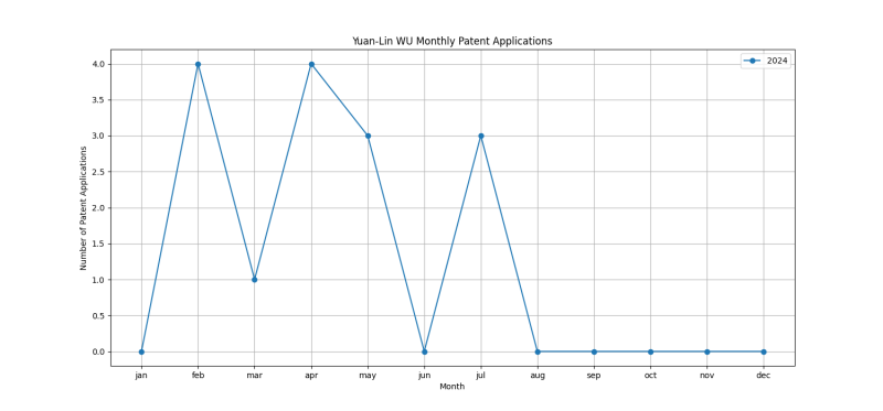
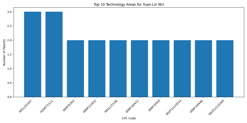
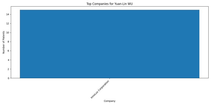
Yuan-Lin WU is an inventor who has filed 15 patents. Their primary areas of innovation include the devices being of types provided for in two or more different main groups of groups (3 patents), ORGANIC ELECTRIC SOLID-STATE DEVICES (3 patents), DISPLAYING; ADVERTISING; SIGNS; LABELS OR NAME-PLATES; SEALS (2 patents), and they have worked with companies such as InnoLux Corporation (15 patents). Their most frequent collaborators include (7 collaborations), (7 collaborations), (3 collaborations).
Patent Filing Activity
Technology Areas
List of Technology Areas
- H01L25/167 (the devices being of types provided for in two or more different main groups of groups): 3 patents
- H10K77/111 (ORGANIC ELECTRIC SOLID-STATE DEVICES): 3 patents
- G09F9/301 (DISPLAYING; ADVERTISING; SIGNS; LABELS OR NAME-PLATES; SEALS): 2 patents
- G06F1/1652 ({the display being flexible, e.g. mimicking a sheet of paper, or rollable}): 2 patents
- H01L27/156 (including semiconductor components having potential barriers, specially adapted for light emission): 2 patents
- G06F3/0412 ({Digitisers structurally integrated in a display}): 2 patents
- G06F3/044 (by capacitive means): 2 patents
- G02F1/133514 ({Colour filters}): 2 patents
- G06F3/0446 ({using a grid-like structure of electrodes in at least two directions, e.g. using row and column electrodes}): 2 patents
- G02F1/133305 (Constructional arrangements; Operation of liquid crystal cells; Circuit arrangements (arrangements or circuits for control of liquid crystal elements in a matrix, not structurally associated with these elements): 2 patents
- H01L27/1218 (the substrate being other than a semiconductor body, e.g. an insulating body): 1 patents
- H01L27/1262 (the substrate being other than a semiconductor body, e.g. an insulating body): 1 patents
- G06F1/206 ({comprising thermal management}): 1 patents
- H05K5/0017 (Casings, cabinets or drawers for electric apparatus): 1 patents
- H05K1/18 (Printed circuits structurally associated with non-printed electric components ({): 1 patents
- H10K39/601 (ORGANIC ELECTRIC SOLID-STATE DEVICES): 1 patents
- H10K59/60 (ORGANIC ELECTRIC SOLID-STATE DEVICES): 1 patents
- A61B5/0059 ({using light, e.g. diagnosis by transillumination, diascopy, fluorescence (): 1 patents
- H01L33/58 (Optical field-shaping elements): 1 patents
- H01L25/0753 (the devices being of a type provided for in group): 1 patents
- H01L31/14 (the light source or sources being controlled by the semiconductor device sensitive to radiation, e.g. image converters, image amplifiers or image storage devices): 1 patents
- H01L31/16 (the semiconductor device sensitive to radiation being controlled by the light source or sources): 1 patents
- H01L33/0012 ({p-i-n devices}): 1 patents
- H01L33/005 ({Processes}): 1 patents
- H01L33/0093 ({Wafer bonding; Removal of the growth substrate}): 1 patents
- H01L33/44 (characterised by the coatings, e.g. passivation layer or anti-reflective coating): 1 patents
- H01L33/48 (characterised by the semiconductor body packages): 1 patents
- H01L33/62 (Arrangements for conducting electric current to or from the semiconductor body, e.g. lead-frames, wire-bonds or solder balls): 1 patents
- G06F3/041662 ({Details of scanning methods, e.g. sampling time, grouping of sub areas or time sharing with display driving (Synchronisation with the driving of the display or the backlighting unit to avoid interferences generated internally): 1 patents
- G06F3/041661 ({Details of scanning methods, e.g. sampling time, grouping of sub areas or time sharing with display driving (Synchronisation with the driving of the display or the backlighting unit to avoid interferences generated internally): 1 patents
- H10K59/40 (ORGANIC ELECTRIC SOLID-STATE DEVICES): 1 patents
- H10K2102/311 (ORGANIC ELECTRIC SOLID-STATE DEVICES): 1 patents
- G02F1/133528 ({Polarisers}): 1 patents
- G02F1/1339 (Constructional arrangements; Operation of liquid crystal cells; Circuit arrangements (arrangements or circuits for control of liquid crystal elements in a matrix, not structurally associated with these elements): 1 patents
- H10K59/50 (ORGANIC ELECTRIC SOLID-STATE DEVICES): 1 patents
- G02F1/133548 (Structural association of cells with optical devices, e.g. polarisers or reflectors): 1 patents
- G02F2201/16 (OPTICAL DEVICES OR ARRANGEMENTS FOR THE CONTROL OF LIGHT BY MODIFICATION OF THE OPTICAL PROPERTIES OF THE MEDIA OF THE ELEMENTS INVOLVED THEREIN; NON-LINEAR OPTICS; FREQUENCY-CHANGING OF LIGHT; OPTICAL LOGIC ELEMENTS; OPTICAL ANALOGUE/DIGITAL CONVERTERS): 1 patents
- G02F2201/50 (OPTICAL DEVICES OR ARRANGEMENTS FOR THE CONTROL OF LIGHT BY MODIFICATION OF THE OPTICAL PROPERTIES OF THE MEDIA OF THE ELEMENTS INVOLVED THEREIN; NON-LINEAR OPTICS; FREQUENCY-CHANGING OF LIGHT; OPTICAL LOGIC ELEMENTS; OPTICAL ANALOGUE/DIGITAL CONVERTERS): 1 patents
- G02F2202/28 (OPTICAL DEVICES OR ARRANGEMENTS FOR THE CONTROL OF LIGHT BY MODIFICATION OF THE OPTICAL PROPERTIES OF THE MEDIA OF THE ELEMENTS INVOLVED THEREIN; NON-LINEAR OPTICS; FREQUENCY-CHANGING OF LIGHT; OPTICAL LOGIC ELEMENTS; OPTICAL ANALOGUE/DIGITAL CONVERTERS): 1 patents
- G06F3/0445 ({using two or more layers of sensing electrodes, e.g. using two layers of electrodes separated by a dielectric layer}): 1 patents
- G06F2203/04107 (ELECTRIC DIGITAL DATA PROCESSING (computer systems based on specific computational models): 1 patents
- G06F3/04166 ({Details of scanning methods, e.g. sampling time, grouping of sub areas or time sharing with display driving (Synchronisation with the driving of the display or the backlighting unit to avoid interferences generated internally): 1 patents
- G06F3/04186 ({Touch location disambiguation}): 1 patents
- G06F3/042 (by opto-electronic means): 1 patents
- G06F3/045 (using resistive elements, e.g. a single continuous surface or two parallel surfaces put in contact): 1 patents
- G06F2203/04102 (ELECTRIC DIGITAL DATA PROCESSING (computer systems based on specific computational models): 1 patents
- G09G3/3266 (Details of drivers for scan electrodes): 1 patents
- G06F3/04164 ({Connections between sensors and controllers, e.g. routing lines between electrodes and connection pads}): 1 patents
- H01L23/544 (Marks applied to semiconductor devices {or parts}, e.g. registration marks, {alignment structures, wafer maps (test patterns for characterising or monitoring manufacturing processes): 1 patents
- H01L27/1225 (the substrate being other than a semiconductor body, e.g. an insulating body): 1 patents
- H01L27/124 (the substrate being other than a semiconductor body, e.g. an insulating body): 1 patents
- H01L27/1251 (the substrate being other than a semiconductor body, e.g. an insulating body): 1 patents
- G09G2310/0297 (ARRANGEMENTS OR CIRCUITS FOR CONTROL OF INDICATING DEVICES USING STATIC MEANS TO PRESENT VARIABLE INFORMATION (arrangements for transferring data between digital computers and displays): 1 patents
- H01L2223/54426 (SEMICONDUCTOR DEVICES NOT COVERED BY CLASS): 1 patents
- H05K5/0018 (Casings, cabinets or drawers for electric apparatus): 1 patents
- G06F1/1637 ({Details related to the display arrangement, including those related to the mounting of the display in the housing}): 1 patents
- H05K5/0217 (PRINTED CIRCUITS; CASINGS OR CONSTRUCTIONAL DETAILS OF ELECTRIC APPARATUS; MANUFACTURE OF ASSEMBLAGES OF ELECTRICAL COMPONENTS): 1 patents
- H01L23/60 (Protection against electrostatic charges or discharges, e.g. Faraday shields): 1 patents
- H04M1/0268 ({including a flexible display panel}): 1 patents
- G09G2330/04 (ARRANGEMENTS OR CIRCUITS FOR CONTROL OF INDICATING DEVICES USING STATIC MEANS TO PRESENT VARIABLE INFORMATION (arrangements for transferring data between digital computers and displays): 1 patents
- H05K3/4688 (Manufacturing multilayer circuits): 1 patents
- H05K1/0306 (Use of materials for the substrate): 1 patents
- H05K3/386 (Improvement of the adhesion between the insulating substrate and the metal): 1 patents
- H05K3/42 (PRINTED CIRCUITS; CASINGS OR CONSTRUCTIONAL DETAILS OF ELECTRIC APPARATUS; MANUFACTURE OF ASSEMBLAGES OF ELECTRICAL COMPONENTS): 1 patents
- H05K2201/09045 (PRINTED CIRCUITS; CASINGS OR CONSTRUCTIONAL DETAILS OF ELECTRIC APPARATUS; MANUFACTURE OF ASSEMBLAGES OF ELECTRICAL COMPONENTS): 1 patents
- H05K2201/20 (PRINTED CIRCUITS; CASINGS OR CONSTRUCTIONAL DETAILS OF ELECTRIC APPARATUS; MANUFACTURE OF ASSEMBLAGES OF ELECTRICAL COMPONENTS): 1 patents
- G02F1/13338 ({Input devices, e.g. touch panels}): 1 patents
- G02F1/136209 (based on liquid crystals, e.g. single liquid crystal display cells): 1 patents
- G02F1/133723 (Constructional arrangements; Operation of liquid crystal cells; Circuit arrangements (arrangements or circuits for control of liquid crystal elements in a matrix, not structurally associated with these elements): 1 patents
- G02F1/136277 (based on liquid crystals, e.g. single liquid crystal display cells): 1 patents
- G02F1/136222 (based on liquid crystals, e.g. single liquid crystal display cells): 1 patents
Companies
List of Companies
- InnoLux Corporation: 15 patents
Collaborators
- Tsung-Han TSAI (7 collaborations)
- Kuan-Feng LEE (7 collaborations)
- Kuan-Feng Lee (3 collaborations)
- Tsung-Han Tsai (2 collaborations)
- Chandra LIUS (2 collaborations)
- Jia-Yuan CHEN (2 collaborations)
- Yu-Chia HUANG (2 collaborations)
- Jui-Jen YUEH (1 collaborations)
- Hsiu-Tung LIN (1 collaborations)
- Chung-Wen YEN (1 collaborations)
Subcategories
This category has the following 8 subcategories, out of 8 total.


