Category:Yasuhito YOSHIMIZU
Jump to navigation
Jump to search
Contents
Yasuhito YOSHIMIZU
Executive Summary
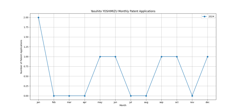
Yasuhito YOSHIMIZU is an inventor who has filed 7 patents. Their primary areas of innovation include SEMICONDUCTOR DEVICES NOT COVERED BY CLASS (3 patents), ELECTRONIC MEMORY DEVICES (3 patents), {the opening being a via or contact hole penetrating the underlying conductor} (2 patents), and they have worked with companies such as Kioxia Corporation (7 patents). Their most frequent collaborators include (4 collaborations), (2 collaborations), (2 collaborations).
Patent Filing Activity
Technology Areas
List of Technology Areas
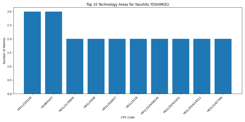
- H01L23/5226 (SEMICONDUCTOR DEVICES NOT COVERED BY CLASS): 3 patents
- H10B43/27 (ELECTRONIC MEMORY DEVICES): 3 patents
- H01L21/76805 ({the opening being a via or contact hole penetrating the underlying conductor}): 2 patents
- H01L24/08 (SEMICONDUCTOR DEVICES NOT COVERED BY CLASS): 2 patents
- H01L25/0657 (SEMICONDUCTOR DEVICES NOT COVERED BY CLASS): 2 patents
- H01L25/18 (the devices being of types provided for in two or more different subgroups of the same main group of groups): 2 patents
- H01L2224/08145 (SEMICONDUCTOR DEVICES NOT COVERED BY CLASS): 2 patents
- H01L2924/1431 (SEMICONDUCTOR DEVICES NOT COVERED BY CLASS): 2 patents
- H01L2924/14511 (SEMICONDUCTOR DEVICES NOT COVERED BY CLASS): 2 patents
- H01L21/67769 (Apparatus specially adapted for handling semiconductor or electric solid state devices during manufacture or treatment thereof; Apparatus specially adapted for handling wafers during manufacture or treatment of semiconductor or electric solid state devices or components {; Apparatus not specifically provided for elsewhere (processes per se): 2 patents
- H01L21/67781 (Apparatus specially adapted for handling semiconductor or electric solid state devices during manufacture or treatment thereof; Apparatus specially adapted for handling wafers during manufacture or treatment of semiconductor or electric solid state devices or components {; Apparatus not specifically provided for elsewhere (processes per se): 2 patents
- H01L21/6773 (Apparatus specially adapted for handling semiconductor or electric solid state devices during manufacture or treatment thereof; Apparatus specially adapted for handling wafers during manufacture or treatment of semiconductor or electric solid state devices or components {; Apparatus not specifically provided for elsewhere (processes per se): 2 patents
- H10B41/27 (ELECTRONIC MEMORY DEVICES): 2 patents
- H01L23/535 (including internal interconnections, e.g. cross-under constructions {(internal lead connections): 1 patents
- H01L21/76895 (Applying interconnections to be used for carrying current between separate components within a device {comprising conductors and dielectrics}): 1 patents
- G11C11/4096 (Input/output [I/O] data management or control circuits, e.g. reading or writing circuits, I/O drivers or bit-line switches): 1 patents
- G11C11/4074 (Power supply or voltage generation circuits, e.g. bias voltage generators, substrate voltage generators, back-up power, power control circuits): 1 patents
- G11C11/4085 ({Word line control circuits, e.g. word line drivers, - boosters, - pull-up, - pull-down, - precharge}): 1 patents
- H01L21/67248 (Apparatus specially adapted for handling semiconductor or electric solid state devices during manufacture or treatment thereof; Apparatus specially adapted for handling wafers during manufacture or treatment of semiconductor or electric solid state devices or components {; Apparatus not specifically provided for elsewhere (processes per se): 1 patents
- G01R1/07314 (Multiple probes): 1 patents
- G01R1/06755 ({Material aspects}): 1 patents
- H01L22/32 (SEMICONDUCTOR DEVICES NOT COVERED BY CLASS): 1 patents
- H01L21/67766 ({Mechanical parts of transfer devices (robots in general in): 1 patents
- H01L21/68 (for positioning, orientation or alignment): 1 patents
- H05K7/20372 (Modifications to facilitate cooling, ventilating, or heating): 1 patents
- H05K7/20381 (Modifications to facilitate cooling, ventilating, or heating): 1 patents
- H01L23/481 (Arrangements for conducting electric current to or from the solid state body in operation, e.g. leads, terminal arrangements {; Selection of materials therefor}): 1 patents
- H01L21/76831 ({in via holes or trenches, e.g. non-conductive sidewall liners}): 1 patents
- H01L21/76834 ({formation of thin insulating films on the sidewalls or on top of conductors (): 1 patents
- H10B43/10 (ELECTRONIC MEMORY DEVICES): 1 patents
Companies
List of Companies
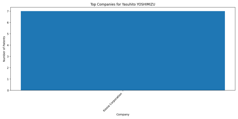
- Kioxia Corporation: 7 patents
Collaborators
- Tomoya SANUKI (4 collaborations)
- Tatsuro HITOMI (2 collaborations)
- Arata INOUE (2 collaborations)
- Hiroyuki DOHMAE (2 collaborations)
- Kazuhito HAYASAKA (2 collaborations)
- Yusuke HIGASHI (1 collaborations)
- Hideko MUKAIDA (1 collaborations)
- Hiroshi NAKAKI (1 collaborations)
- Yoshiro SHIMOJO (1 collaborations)
- Shinya ARAI (1 collaborations)
Subcategories
This category has the following 2 subcategories, out of 2 total.


