Category:Tomoya SANUKI
Jump to navigation
Jump to search
Contents
Tomoya SANUKI
Executive Summary
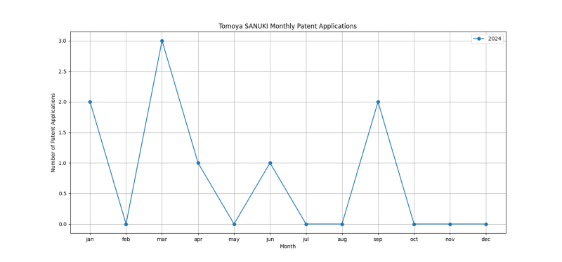
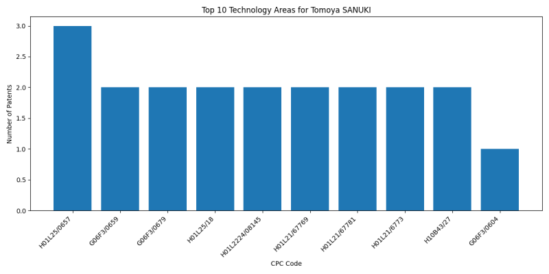
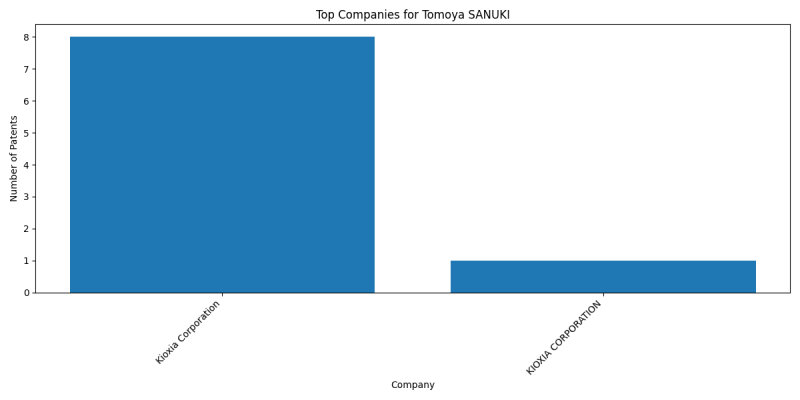
Tomoya SANUKI is an inventor who has filed 9 patents. Their primary areas of innovation include SEMICONDUCTOR DEVICES NOT COVERED BY CLASS (3 patents), {Command handling arrangements, e.g. command buffers, queues, command scheduling} (2 patents), {Non-volatile semiconductor memory device, e.g. flash memory, one time programmable memory [OTP]} (2 patents), and they have worked with companies such as Kioxia Corporation (8 patents), KIOXIA CORPORATION (1 patents). Their most frequent collaborators include (4 collaborations), (2 collaborations), (2 collaborations).
Patent Filing Activity
Technology Areas
List of Technology Areas
- H01L25/0657 (SEMICONDUCTOR DEVICES NOT COVERED BY CLASS): 3 patents
- G06F3/0659 ({Command handling arrangements, e.g. command buffers, queues, command scheduling}): 2 patents
- G06F3/0679 ({Non-volatile semiconductor memory device, e.g. flash memory, one time programmable memory [OTP]}): 2 patents
- H01L25/18 (the devices being of types provided for in two or more different subgroups of the same main group of groups): 2 patents
- H01L2224/08145 (SEMICONDUCTOR DEVICES NOT COVERED BY CLASS): 2 patents
- H01L21/67769 (Apparatus specially adapted for handling semiconductor or electric solid state devices during manufacture or treatment thereof; Apparatus specially adapted for handling wafers during manufacture or treatment of semiconductor or electric solid state devices or components {; Apparatus not specifically provided for elsewhere (processes per se): 2 patents
- H01L21/67781 (Apparatus specially adapted for handling semiconductor or electric solid state devices during manufacture or treatment thereof; Apparatus specially adapted for handling wafers during manufacture or treatment of semiconductor or electric solid state devices or components {; Apparatus not specifically provided for elsewhere (processes per se): 2 patents
- H01L21/6773 (Apparatus specially adapted for handling semiconductor or electric solid state devices during manufacture or treatment thereof; Apparatus specially adapted for handling wafers during manufacture or treatment of semiconductor or electric solid state devices or components {; Apparatus not specifically provided for elsewhere (processes per se): 2 patents
- H10B43/27 (ELECTRONIC MEMORY DEVICES): 2 patents
- G06F3/0604 (Digital input from, or digital output to, record carriers {, e.g. RAID, emulated record carriers or networked record carriers}): 1 patents
- G06F3/0634 ({by changing the state or mode of one or more devices}): 1 patents
- G11C11/4096 (Input/output [I/O] data management or control circuits, e.g. reading or writing circuits, I/O drivers or bit-line switches): 1 patents
- G11C11/4074 (Power supply or voltage generation circuits, e.g. bias voltage generators, substrate voltage generators, back-up power, power control circuits): 1 patents
- G11C11/4085 ({Word line control circuits, e.g. word line drivers, - boosters, - pull-up, - pull-down, - precharge}): 1 patents
- H01L24/08 (SEMICONDUCTOR DEVICES NOT COVERED BY CLASS): 1 patents
- H01L2225/06524 (SEMICONDUCTOR DEVICES NOT COVERED BY CLASS): 1 patents
- H01L2225/06593 (SEMICONDUCTOR DEVICES NOT COVERED BY CLASS): 1 patents
- H01L2225/06596 (SEMICONDUCTOR DEVICES NOT COVERED BY CLASS): 1 patents
- H01L2924/1431 (SEMICONDUCTOR DEVICES NOT COVERED BY CLASS): 1 patents
- H01L2924/14511 (SEMICONDUCTOR DEVICES NOT COVERED BY CLASS): 1 patents
- H01L21/67248 (Apparatus specially adapted for handling semiconductor or electric solid state devices during manufacture or treatment thereof; Apparatus specially adapted for handling wafers during manufacture or treatment of semiconductor or electric solid state devices or components {; Apparatus not specifically provided for elsewhere (processes per se): 1 patents
- G01R1/07314 (Multiple probes): 1 patents
- G01R1/06755 ({Material aspects}): 1 patents
- H01L22/32 (SEMICONDUCTOR DEVICES NOT COVERED BY CLASS): 1 patents
- H01L21/67766 ({Mechanical parts of transfer devices (robots in general in): 1 patents
- H01L21/68 (for positioning, orientation or alignment): 1 patents
- H05K7/20372 (Modifications to facilitate cooling, ventilating, or heating): 1 patents
- H05K7/20381 (Modifications to facilitate cooling, ventilating, or heating): 1 patents
- G11C5/063 (STATIC STORES (semiconductor memory devices): 1 patents
- H01L24/09 (SEMICONDUCTOR DEVICES NOT COVERED BY CLASS): 1 patents
- H10B43/40 (ELECTRONIC MEMORY DEVICES): 1 patents
- H01L21/185 ({Joining of semiconductor bodies for junction formation}): 1 patents
- H01L21/76898 ({formed through a semiconductor substrate}): 1 patents
- H01L24/80 ({Methods for connecting semiconductor or other solid state bodies using means for bonding being attached to, or being formed on, the surface to be connected}): 1 patents
- H10B43/30 (ELECTRONIC MEMORY DEVICES): 1 patents
- H10B43/50 (ELECTRONIC MEMORY DEVICES): 1 patents
- G06F3/0619 ({in relation to data integrity, e.g. data losses, bit errors}): 1 patents
Companies
List of Companies
- Kioxia Corporation: 8 patents
- KIOXIA CORPORATION: 1 patents
Collaborators
- Yasuhito YOSHIMIZU (4 collaborations)
- Tatsuro HITOMI (2 collaborations)
- Arata INOUE (2 collaborations)
- Hiroyuki DOHMAE (2 collaborations)
- Kazuhito HAYASAKA (2 collaborations)
- Yoshihiro OHBA (1 collaborations)
- Takeshi ISHIHARA (1 collaborations)
- Hiroshi MAEJIMA (1 collaborations)
- Tetsuaki UTSUMI (1 collaborations)
- Yusuke HIGASHI (1 collaborations)
- Hideko MUKAIDA (1 collaborations)
- Yoshiaki FUKUZUMI (1 collaborations)
- Hideaki AOCHI (1 collaborations)
- Mie MATSUO (1 collaborations)
- Kenichiro YOSHII (1 collaborations)
- Koichiro SHINDO (1 collaborations)
- Kazushige KAWASAKI (1 collaborations)
- Toshio FUJISAWA (1 collaborations)
- Keisuke NAKATSUKA (1 collaborations)
Subcategories
This category has the following 3 subcategories, out of 3 total.
Categories:
- Yasuhito YOSHIMIZU
- Tatsuro HITOMI
- Arata INOUE
- Hiroyuki DOHMAE
- Kazuhito HAYASAKA
- Yoshihiro OHBA
- Takeshi ISHIHARA
- Hiroshi MAEJIMA
- Tetsuaki UTSUMI
- Yusuke HIGASHI
- Hideko MUKAIDA
- Yoshiaki FUKUZUMI
- Hideaki AOCHI
- Mie MATSUO
- Kenichiro YOSHII
- Koichiro SHINDO
- Kazushige KAWASAKI
- Toshio FUJISAWA
- Keisuke NAKATSUKA
- Tomoya SANUKI
- Inventors
- Inventors filing patents with Kioxia Corporation
- Inventors filing patents with KIOXIA CORPORATION


