Category:Shinichiro OKA
Jump to navigation
Jump to search
Contents
Shinichiro OKA
Executive Summary
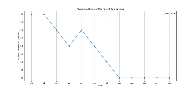
Shinichiro OKA is an inventor who has filed 19 patents. Their primary areas of innovation include with variable phase-shifters (3 patents), {with means for varying the reflecting properties ( (3 patents), based on liquid crystals, e.g. single liquid crystal display cells (3 patents), and they have worked with companies such as Japan Display Inc. (19 patents). Their most frequent collaborators include (8 collaborations), (7 collaborations), (7 collaborations).
Patent Filing Activity
Technology Areas
List of Technology Areas
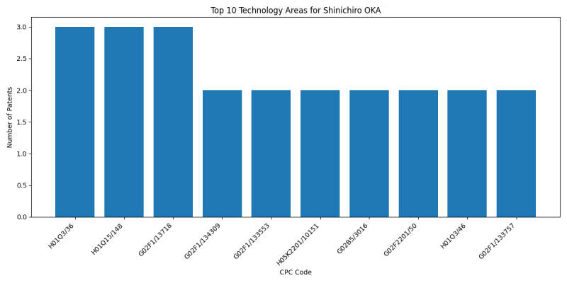
- H01Q3/36 (with variable phase-shifters): 3 patents
- H01Q15/148 ({with means for varying the reflecting properties (): 3 patents
- G02F1/13718 (based on liquid crystals, e.g. single liquid crystal display cells): 3 patents
- G02F1/134309 ({characterised by their geometrical arrangement}): 2 patents
- G02F1/133553 (Structural association of cells with optical devices, e.g. polarisers or reflectors): 2 patents
- H05K2201/10151 (PRINTED CIRCUITS; CASINGS OR CONSTRUCTIONAL DETAILS OF ELECTRIC APPARATUS; MANUFACTURE OF ASSEMBLAGES OF ELECTRICAL COMPONENTS): 2 patents
- G02B5/3016 (OPTICAL ELEMENTS, SYSTEMS OR APPARATUS): 2 patents
- G02F2201/50 (OPTICAL DEVICES OR ARRANGEMENTS FOR THE CONTROL OF LIGHT BY MODIFICATION OF THE OPTICAL PROPERTIES OF THE MEDIA OF THE ELEMENTS INVOLVED THEREIN; NON-LINEAR OPTICS; FREQUENCY-CHANGING OF LIGHT; OPTICAL LOGIC ELEMENTS; OPTICAL ANALOGUE/DIGITAL CONVERTERS): 2 patents
- H01Q3/46 (Active lenses or reflecting arrays): 2 patents
- G02F1/133757 (Constructional arrangements; Operation of liquid crystal cells; Circuit arrangements (arrangements or circuits for control of liquid crystal elements in a matrix, not structurally associated with these elements): 2 patents
- G02F1/133788 (Constructional arrangements; Operation of liquid crystal cells; Circuit arrangements (arrangements or circuits for control of liquid crystal elements in a matrix, not structurally associated with these elements): 2 patents
- G02F1/13478 (Arrangement of liquid crystal layers or cells in which the final condition of one light beam is achieved by the addition of the effects of two or more layers or cells): 2 patents
- H01Q15/0013 ({said selective devices working as frequency-selective reflecting surfaces, e.g. FSS, dichroic plates, surfaces being partly transmissive and reflective}): 1 patents
- H01Q15/14 (Reflecting surfaces; Equivalent structures {(electromagnetic shields): 1 patents
- H01Q17/00 (Devices for absorbing waves radiated from an antenna; Combinations of such devices with active antenna elements or systems): 1 patents
- H01Q21/245 ({provided with means for varying the polarisation (polarising devices): 1 patents
- H05K1/0283 (PRINTED CIRCUITS; CASINGS OR CONSTRUCTIONAL DETAILS OF ELECTRIC APPARATUS; MANUFACTURE OF ASSEMBLAGES OF ELECTRICAL COMPONENTS): 1 patents
- H10K30/87 (ORGANIC ELECTRIC SOLID-STATE DEVICES): 1 patents
- H10K30/50 (ORGANIC ELECTRIC SOLID-STATE DEVICES): 1 patents
- G02F1/133753 (Constructional arrangements; Operation of liquid crystal cells; Circuit arrangements (arrangements or circuits for control of liquid crystal elements in a matrix, not structurally associated with these elements): 1 patents
- H05K1/032 (Use of materials for the substrate): 1 patents
- H05K1/0306 (Use of materials for the substrate): 1 patents
- H05K1/118 (PRINTED CIRCUITS; CASINGS OR CONSTRUCTIONAL DETAILS OF ELECTRIC APPARATUS; MANUFACTURE OF ASSEMBLAGES OF ELECTRICAL COMPONENTS): 1 patents
- H05K3/103 (PRINTED CIRCUITS; CASINGS OR CONSTRUCTIONAL DETAILS OF ELECTRIC APPARATUS; MANUFACTURE OF ASSEMBLAGES OF ELECTRICAL COMPONENTS): 1 patents
- H05K2201/10106 (PRINTED CIRCUITS; CASINGS OR CONSTRUCTIONAL DETAILS OF ELECTRIC APPARATUS; MANUFACTURE OF ASSEMBLAGES OF ELECTRICAL COMPONENTS): 1 patents
- H01L31/0543 (Optical elements directly associated or integrated with the PV cell, e.g. light-reflecting means or light-concentrating means): 1 patents
- G02F1/1396 (based on liquid crystals, e.g. single liquid crystal display cells): 1 patents
- G02F1/13471 (Arrangement of liquid crystal layers or cells in which the final condition of one light beam is achieved by the addition of the effects of two or more layers or cells): 1 patents
- G02B6/2726 (with polarisation selective and adjusting means): 1 patents
- G02F1/1347 (Arrangement of liquid crystal layers or cells in which the final condition of one light beam is achieved by the addition of the effects of two or more layers or cells): 1 patents
- G02F1/011 ({in optical waveguides, not otherwise provided for in this subclass}): 1 patents
- G02F1/133711 (Constructional arrangements; Operation of liquid crystal cells; Circuit arrangements (arrangements or circuits for control of liquid crystal elements in a matrix, not structurally associated with these elements): 1 patents
- G02F1/133784 (Constructional arrangements; Operation of liquid crystal cells; Circuit arrangements (arrangements or circuits for control of liquid crystal elements in a matrix, not structurally associated with these elements): 1 patents
- G02F1/133761 (Constructional arrangements; Operation of liquid crystal cells; Circuit arrangements (arrangements or circuits for control of liquid crystal elements in a matrix, not structurally associated with these elements): 1 patents
- G02F1/133365 ({Cells in which the active layer comprises a liquid crystalline polymer}): 1 patents
- G02F1/133536 (Structural association of cells with optical devices, e.g. polarisers or reflectors): 1 patents
- B32B27/281 (LAYERED PRODUCTS, i.e. PRODUCTS BUILT-UP OF STRATA OF FLAT OR NON-FLAT, e.g. CELLULAR OR HONEYCOMB, FORM): 1 patents
- B32B27/308 (comprising vinyl {(co)polymers; comprising acrylic (co)polymers}): 1 patents
- B32B27/06 (LAYERED PRODUCTS, i.e. PRODUCTS BUILT-UP OF STRATA OF FLAT OR NON-FLAT, e.g. CELLULAR OR HONEYCOMB, FORM): 1 patents
- B32B2307/206 (LAYERED PRODUCTS, i.e. PRODUCTS BUILT-UP OF STRATA OF FLAT OR NON-FLAT, e.g. CELLULAR OR HONEYCOMB, FORM): 1 patents
- B32B2307/204 (LAYERED PRODUCTS, i.e. PRODUCTS BUILT-UP OF STRATA OF FLAT OR NON-FLAT, e.g. CELLULAR OR HONEYCOMB, FORM): 1 patents
- G02F1/134381 (based on liquid crystals, e.g. single liquid crystal display cells): 1 patents
- G02F1/13439 (based on liquid crystals, e.g. single liquid crystal display cells): 1 patents
- G02F1/1368 (based on liquid crystals, e.g. single liquid crystal display cells): 1 patents
- G02F2203/02 (OPTICAL DEVICES OR ARRANGEMENTS FOR THE CONTROL OF LIGHT BY MODIFICATION OF THE OPTICAL PROPERTIES OF THE MEDIA OF THE ELEMENTS INVOLVED THEREIN; NON-LINEAR OPTICS; FREQUENCY-CHANGING OF LIGHT; OPTICAL LOGIC ELEMENTS; OPTICAL ANALOGUE/DIGITAL CONVERTERS): 1 patents
- H01L33/325 ({characterised by the doping materials}): 1 patents
- C23C14/0641 (COATING METALLIC MATERIAL; COATING MATERIAL WITH METALLIC MATERIAL; SURFACE TREATMENT OF METALLIC MATERIAL BY DIFFUSION INTO THE SURFACE, BY CHEMICAL CONVERSION OR SUBSTITUTION; COATING BY VACUUM EVAPORATION, BY SPUTTERING, BY ION IMPLANTATION OR BY CHEMICAL VAPOUR DEPOSITION, IN GENERAL (making metal-coated products by extrusion): 1 patents
- H01L33/22 (Roughened surfaces, e.g. at the interface between epitaxial layers): 1 patents
- G02F1/133726 (Constructional arrangements; Operation of liquid crystal cells; Circuit arrangements (arrangements or circuits for control of liquid crystal elements in a matrix, not structurally associated with these elements): 1 patents
- H01L31/054 (Optical elements directly associated or integrated with the PV cell, e.g. light-reflecting means or light-concentrating means): 1 patents
- H01Q21/065 ({Patch antenna array}): 1 patents
Companies
List of Companies
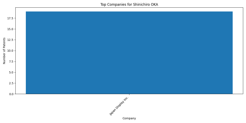
- Japan Display Inc.: 19 patents
Collaborators
- Mitsutaka OKITA (8 collaborations)
- Shigesumi ARAKI (7 collaborations)
- Daiichi SUZUKI (7 collaborations)
- Yasushi TOMIOKA (7 collaborations)
- Koichi IGETA (7 collaborations)
- Junji KOBASHI (6 collaborations)
- Hiroumi KINJO (3 collaborations)
- Hiroyuki YOSHIDA (3 collaborations)
- Yoshiaki AMANO (3 collaborations)
- Hiromi MATSUNO (3 collaborations)
- Takumi SANO (2 collaborations)
- Masatomo HISHINUMA (2 collaborations)
- Akio MURAYAMA (2 collaborations)
- Yasuyuki YAMADA (1 collaborations)
- Masumi NISHIMURA (1 collaborations)
- Hayata AOKI (1 collaborations)
- Ayaka HIGUCHI (1 collaborations)
Subcategories
This category has the following 7 subcategories, out of 7 total.
H
J
K
M
S
T
Y
Categories:
- Mitsutaka OKITA
- Shigesumi ARAKI
- Daiichi SUZUKI
- Yasushi TOMIOKA
- Koichi IGETA
- Junji KOBASHI
- Hiroumi KINJO
- Hiroyuki YOSHIDA
- Yoshiaki AMANO
- Hiromi MATSUNO
- Takumi SANO
- Masatomo HISHINUMA
- Akio MURAYAMA
- Yasuyuki YAMADA
- Masumi NISHIMURA
- Hayata AOKI
- Ayaka HIGUCHI
- Shinichiro OKA
- Inventors
- Inventors filing patents with Japan Display Inc.


