Category:Shin-Puu Jeng
Jump to navigation
Jump to search
Contents
Shin-Puu Jeng
Executive Summary
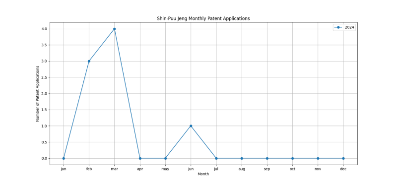
Shin-Puu Jeng is an inventor who has filed 8 patents. Their primary areas of innovation include SEMICONDUCTOR DEVICES NOT COVERED BY CLASS (4 patents), SEMICONDUCTOR DEVICES NOT COVERED BY CLASS (4 patents), Manufacture or treatment of parts, e.g. containers, prior to assembly of the devices, using processes not provided for in a single one of the subgroups (4 patents), and they have worked with companies such as Taiwan Semiconductor Manufacturing Co., Ltd. (8 patents). Their most frequent collaborators include (3 collaborations), (3 collaborations), (2 collaborations).
Patent Filing Activity
Technology Areas
List of Technology Areas
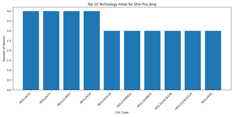
- H01L24/32 (SEMICONDUCTOR DEVICES NOT COVERED BY CLASS): 4 patents
- H01L24/73 (SEMICONDUCTOR DEVICES NOT COVERED BY CLASS): 4 patents
- H01L21/4857 (Manufacture or treatment of parts, e.g. containers, prior to assembly of the devices, using processes not provided for in a single one of the subgroups): 4 patents
- H01L24/16 (SEMICONDUCTOR DEVICES NOT COVERED BY CLASS): 4 patents
- H01L23/3128 (SEMICONDUCTOR DEVICES NOT COVERED BY CLASS): 3 patents
- H01L23/49822 ({Multilayer substrates (multilayer metallisation on monolayer substrate): 3 patents
- H01L23/49833 (Leads, {i.e. metallisations or lead-frames} on insulating substrates, {e.g. chip carriers (shape of the substrate): 3 patents
- H01L2224/16238 (SEMICONDUCTOR DEVICES NOT COVERED BY CLASS): 3 patents
- H01L2224/32225 (SEMICONDUCTOR DEVICES NOT COVERED BY CLASS): 3 patents
- H01L24/81 (SEMICONDUCTOR DEVICES NOT COVERED BY CLASS): 3 patents
- H01L25/50 ({Multistep manufacturing processes of assemblies consisting of devices, each device being of a type provided for in group): 3 patents
- H01L23/3185 (SEMICONDUCTOR DEVICES NOT COVERED BY CLASS): 3 patents
- H01L24/09 (SEMICONDUCTOR DEVICES NOT COVERED BY CLASS): 2 patents
- H01L24/17 (SEMICONDUCTOR DEVICES NOT COVERED BY CLASS): 2 patents
- H01L21/4853 (Manufacture or treatment of parts, e.g. containers, prior to assembly of the devices, using processes not provided for in a single one of the subgroups): 2 patents
- H01L23/49838 (Leads, {i.e. metallisations or lead-frames} on insulating substrates, {e.g. chip carriers (shape of the substrate): 2 patents
- H01L24/96 ({the devices being encapsulated in a common layer, e.g. neo-wafer or pseudo-wafer, said common layer being separable into individual assemblies after connecting}): 2 patents
- H01L2224/16227 (SEMICONDUCTOR DEVICES NOT COVERED BY CLASS): 2 patents
- H01L2224/73204 (SEMICONDUCTOR DEVICES NOT COVERED BY CLASS): 2 patents
- H01L2224/95001 (SEMICONDUCTOR DEVICES NOT COVERED BY CLASS): 2 patents
- H01L2924/15311 (SEMICONDUCTOR DEVICES NOT COVERED BY CLASS): 2 patents
- H01L24/13 (SEMICONDUCTOR DEVICES NOT COVERED BY CLASS): 2 patents
- H01L2224/81815 (SEMICONDUCTOR DEVICES NOT COVERED BY CLASS): 2 patents
- H01L21/568 (SEMICONDUCTOR DEVICES NOT COVERED BY CLASS): 2 patents
- H01L23/5383 ({Multilayer substrates (): 2 patents
- H01L24/19 (SEMICONDUCTOR DEVICES NOT COVERED BY CLASS): 2 patents
- H01L24/20 (SEMICONDUCTOR DEVICES NOT COVERED BY CLASS): 2 patents
- H01L23/562 (SEMICONDUCTOR DEVICES NOT COVERED BY CLASS): 2 patents
- H01L23/481 (Arrangements for conducting electric current to or from the solid state body in operation, e.g. leads, terminal arrangements {; Selection of materials therefor}): 2 patents
- H01L23/5386 (the interconnection structure between a plurality of semiconductor chips being formed on, or in, insulating substrates ({): 2 patents
- H01L23/5389 (the interconnection structure between a plurality of semiconductor chips being formed on, or in, insulating substrates ({): 2 patents
- H01L25/0657 (SEMICONDUCTOR DEVICES NOT COVERED BY CLASS): 2 patents
- H01L2224/12105 (SEMICONDUCTOR DEVICES NOT COVERED BY CLASS): 2 patents
- H01L25/18 (the devices being of types provided for in two or more different subgroups of the same main group of groups): 1 patents
- H01L21/566 (SEMICONDUCTOR DEVICES NOT COVERED BY CLASS): 1 patents
- H01L23/3114 (SEMICONDUCTOR DEVICES NOT COVERED BY CLASS): 1 patents
- H01L2224/0231 (SEMICONDUCTOR DEVICES NOT COVERED BY CLASS): 1 patents
- H01L2224/02379 (SEMICONDUCTOR DEVICES NOT COVERED BY CLASS): 1 patents
- H01L2224/0401 (SEMICONDUCTOR DEVICES NOT COVERED BY CLASS): 1 patents
- H01L23/66 (SEMICONDUCTOR DEVICES NOT COVERED BY CLASS): 1 patents
- H01L21/486 (Manufacture or treatment of parts, e.g. containers, prior to assembly of the devices, using processes not provided for in a single one of the subgroups): 1 patents
- H01L23/49816 (Leads, {i.e. metallisations or lead-frames} on insulating substrates, {e.g. chip carriers (shape of the substrate): 1 patents
- H01L23/552 (Protection against radiation, e.g. light {or electromagnetic waves}): 1 patents
- H01L24/97 (SEMICONDUCTOR DEVICES NOT COVERED BY CLASS): 1 patents
- H10B80/00 (Assemblies of multiple devices comprising at least one memory device covered by this subclass): 1 patents
- H01L2223/6616 (SEMICONDUCTOR DEVICES NOT COVERED BY CLASS): 1 patents
- H01L2223/6672 (SEMICONDUCTOR DEVICES NOT COVERED BY CLASS): 1 patents
- H01L2224/96 (SEMICONDUCTOR DEVICES NOT COVERED BY CLASS): 1 patents
- H01L2224/97 (SEMICONDUCTOR DEVICES NOT COVERED BY CLASS): 1 patents
- H01L2924/15174 (SEMICONDUCTOR DEVICES NOT COVERED BY CLASS): 1 patents
- H01L23/3121 (SEMICONDUCTOR DEVICES NOT COVERED BY CLASS): 1 patents
- H01L23/3735 (SEMICONDUCTOR DEVICES NOT COVERED BY CLASS): 1 patents
- H01L2224/13111 (SEMICONDUCTOR DEVICES NOT COVERED BY CLASS): 1 patents
- H01L2224/13139 (SEMICONDUCTOR DEVICES NOT COVERED BY CLASS): 1 patents
- H01L2224/13147 (SEMICONDUCTOR DEVICES NOT COVERED BY CLASS): 1 patents
- H01L2224/81193 (SEMICONDUCTOR DEVICES NOT COVERED BY CLASS): 1 patents
- H01L2924/1517 (SEMICONDUCTOR DEVICES NOT COVERED BY CLASS): 1 patents
- H01L2924/3511 (SEMICONDUCTOR DEVICES NOT COVERED BY CLASS): 1 patents
- H01L25/0652 (SEMICONDUCTOR DEVICES NOT COVERED BY CLASS): 1 patents
- H01L23/3135 (SEMICONDUCTOR DEVICES NOT COVERED BY CLASS): 1 patents
- H01L23/5385 (the interconnection structure between a plurality of semiconductor chips being formed on, or in, insulating substrates ({): 1 patents
- H01L25/0655 (SEMICONDUCTOR DEVICES NOT COVERED BY CLASS): 1 patents
- H01L24/83 (SEMICONDUCTOR DEVICES NOT COVERED BY CLASS): 1 patents
- H01L21/561 (SEMICONDUCTOR DEVICES NOT COVERED BY CLASS): 1 patents
- H01L23/3192 (SEMICONDUCTOR DEVICES NOT COVERED BY CLASS): 1 patents
- H01L24/95 (SEMICONDUCTOR DEVICES NOT COVERED BY CLASS): 1 patents
- H01L24/92 (SEMICONDUCTOR DEVICES NOT COVERED BY CLASS): 1 patents
- H01L2224/19 (SEMICONDUCTOR DEVICES NOT COVERED BY CLASS): 1 patents
- H01L2224/2101 (SEMICONDUCTOR DEVICES NOT COVERED BY CLASS): 1 patents
- H01L2224/215 (SEMICONDUCTOR DEVICES NOT COVERED BY CLASS): 1 patents
- H01L2224/83102 (SEMICONDUCTOR DEVICES NOT COVERED BY CLASS): 1 patents
- H01L23/49894 (Leads, {i.e. metallisations or lead-frames} on insulating substrates, {e.g. chip carriers (shape of the substrate): 1 patents
- H01L2224/92125 (SEMICONDUCTOR DEVICES NOT COVERED BY CLASS): 1 patents
- H01L21/563 (SEMICONDUCTOR DEVICES NOT COVERED BY CLASS): 1 patents
- H01L23/3107 (SEMICONDUCTOR DEVICES NOT COVERED BY CLASS): 1 patents
- H01L2924/18161 (SEMICONDUCTOR DEVICES NOT COVERED BY CLASS): 1 patents
- H01L2924/351 (SEMICONDUCTOR DEVICES NOT COVERED BY CLASS): 1 patents
- H01L2924/35121 (SEMICONDUCTOR DEVICES NOT COVERED BY CLASS): 1 patents
- H01L23/50 (for integrated circuit devices, {e.g. power bus, number of leads} (): 1 patents
- H01L25/105 (SEMICONDUCTOR DEVICES NOT COVERED BY CLASS): 1 patents
- H01L24/48 (SEMICONDUCTOR DEVICES NOT COVERED BY CLASS): 1 patents
- H01L2224/04042 (SEMICONDUCTOR DEVICES NOT COVERED BY CLASS): 1 patents
- H01L2224/04105 (SEMICONDUCTOR DEVICES NOT COVERED BY CLASS): 1 patents
- H01L2224/48091 (SEMICONDUCTOR DEVICES NOT COVERED BY CLASS): 1 patents
- H01L2224/48227 (SEMICONDUCTOR DEVICES NOT COVERED BY CLASS): 1 patents
- H01L2224/73265 (SEMICONDUCTOR DEVICES NOT COVERED BY CLASS): 1 patents
- H01L2224/73267 (SEMICONDUCTOR DEVICES NOT COVERED BY CLASS): 1 patents
- H01L2224/81385 (SEMICONDUCTOR DEVICES NOT COVERED BY CLASS): 1 patents
- H01L2225/1035 (SEMICONDUCTOR DEVICES NOT COVERED BY CLASS): 1 patents
- H01L2225/1041 (SEMICONDUCTOR DEVICES NOT COVERED BY CLASS): 1 patents
- H01L2225/1058 (SEMICONDUCTOR DEVICES NOT COVERED BY CLASS): 1 patents
- H01L2924/00014 (SEMICONDUCTOR DEVICES NOT COVERED BY CLASS): 1 patents
- H01L2924/14 (SEMICONDUCTOR DEVICES NOT COVERED BY CLASS): 1 patents
- H01L2924/1431 (SEMICONDUCTOR DEVICES NOT COVERED BY CLASS): 1 patents
- H01L2924/181 (SEMICONDUCTOR DEVICES NOT COVERED BY CLASS): 1 patents
Companies
List of Companies
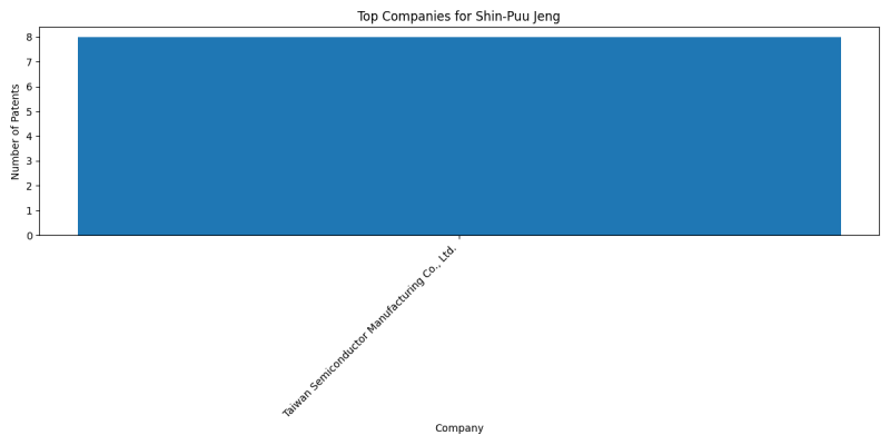
- Taiwan Semiconductor Manufacturing Co., Ltd.: 8 patents
Collaborators
- Meng-Liang Lin (3 collaborations)
- Hsien-Wei Chen (3 collaborations)
- Po-Yao Chuang (2 collaborations)
- Chieh-Lung Lai (2 collaborations)
- Po-Yao Lin (2 collaborations)
- Shu-Shen Yeh (2 collaborations)
- Po-Hao Tsai (1 collaborations)
- Techi Wong (1 collaborations)
- Meng-Wei Chou (1 collaborations)
- Chun-Yueh Yang (1 collaborations)
- Chien-Sheng Chen (1 collaborations)
- Po-Chen Lai (1 collaborations)
- Shuo-Mao Chen (1 collaborations)
- Tsung-Yen Lee (1 collaborations)
- Chia-Kuei Hsu (1 collaborations)
- Ming-Chih Yew (1 collaborations)
- Che-Chia Yang (1 collaborations)
- Chin-Hua Wang (1 collaborations)
- Chia-Hsiang Lin (1 collaborations)
- Chen-Hua Yu (1 collaborations)
- Der-Chyang Yeh (1 collaborations)
- Jie Chen (1 collaborations)
Subcategories
This category has the following 5 subcategories, out of 5 total.
C
H
M
S
Categories:
- Meng-Liang Lin
- Hsien-Wei Chen
- Po-Yao Chuang
- Chieh-Lung Lai
- Po-Yao Lin
- Shu-Shen Yeh
- Po-Hao Tsai
- Techi Wong
- Meng-Wei Chou
- Chun-Yueh Yang
- Chien-Sheng Chen
- Po-Chen Lai
- Shuo-Mao Chen
- Tsung-Yen Lee
- Chia-Kuei Hsu
- Ming-Chih Yew
- Che-Chia Yang
- Chin-Hua Wang
- Chia-Hsiang Lin
- Chen-Hua Yu
- Der-Chyang Yeh
- Jie Chen
- Shin-Puu Jeng
- Inventors
- Inventors filing patents with Taiwan Semiconductor Manufacturing Co., Ltd.


