Category:Shin-Puu JENG
Jump to navigation
Jump to search
Contents
Shin-Puu JENG
Executive Summary
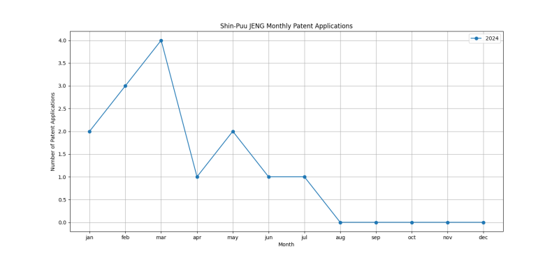
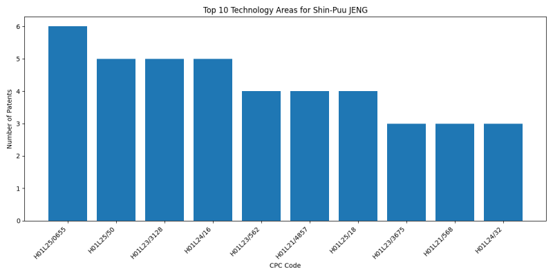
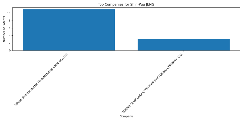
Shin-Puu JENG is an inventor who has filed 14 patents. Their primary areas of innovation include SEMICONDUCTOR DEVICES NOT COVERED BY CLASS (6 patents), {Multistep manufacturing processes of assemblies consisting of devices, each device being of a type provided for in group (5 patents), SEMICONDUCTOR DEVICES NOT COVERED BY CLASS (5 patents), and they have worked with companies such as Taiwan Semiconductor Manufacturing Company, Ltd. (11 patents), TAIWAN SEMICONDUCTOR MANUFACTURING COMPANY, LTD. (3 patents). Their most frequent collaborators include (10 collaborations), (9 collaborations), (8 collaborations).
Patent Filing Activity
Technology Areas
List of Technology Areas
- H01L25/0655 (SEMICONDUCTOR DEVICES NOT COVERED BY CLASS): 6 patents
- H01L25/50 ({Multistep manufacturing processes of assemblies consisting of devices, each device being of a type provided for in group): 5 patents
- H01L23/3128 (SEMICONDUCTOR DEVICES NOT COVERED BY CLASS): 5 patents
- H01L24/16 (SEMICONDUCTOR DEVICES NOT COVERED BY CLASS): 5 patents
- H01L23/562 (SEMICONDUCTOR DEVICES NOT COVERED BY CLASS): 4 patents
- H01L21/4857 (Manufacture or treatment of parts, e.g. containers, prior to assembly of the devices, using processes not provided for in a single one of the subgroups): 4 patents
- H01L25/18 (the devices being of types provided for in two or more different subgroups of the same main group of groups): 4 patents
- H01L23/3675 (Cooling facilitated by shape of device {(): 3 patents
- H01L21/568 (SEMICONDUCTOR DEVICES NOT COVERED BY CLASS): 3 patents
- H01L24/32 (SEMICONDUCTOR DEVICES NOT COVERED BY CLASS): 3 patents
- H01L21/6835 ({using temporarily an auxiliary support}): 3 patents
- H01L23/5383 ({Multilayer substrates (): 3 patents
- H01L21/563 (SEMICONDUCTOR DEVICES NOT COVERED BY CLASS): 3 patents
- H01L23/04 (SEMICONDUCTOR DEVICES NOT COVERED BY CLASS): 2 patents
- H01L23/10 (SEMICONDUCTOR DEVICES NOT COVERED BY CLASS): 2 patents
- H01L23/367 (Cooling facilitated by shape of device {(): 2 patents
- H01L23/49816 (Leads, {i.e. metallisations or lead-frames} on insulating substrates, {e.g. chip carriers (shape of the substrate): 2 patents
- H01L25/0652 (SEMICONDUCTOR DEVICES NOT COVERED BY CLASS): 2 patents
- H01L25/105 (SEMICONDUCTOR DEVICES NOT COVERED BY CLASS): 2 patents
- H01L21/56 (SEMICONDUCTOR DEVICES NOT COVERED BY CLASS): 2 patents
- H01L23/3135 (SEMICONDUCTOR DEVICES NOT COVERED BY CLASS): 2 patents
- H01L21/4853 (Manufacture or treatment of parts, e.g. containers, prior to assembly of the devices, using processes not provided for in a single one of the subgroups): 2 patents
- H01L23/13 (SEMICONDUCTOR DEVICES NOT COVERED BY CLASS): 2 patents
- H01L23/5386 (the interconnection structure between a plurality of semiconductor chips being formed on, or in, insulating substrates ({): 2 patents
- H01L2221/68372 (SEMICONDUCTOR DEVICES NOT COVERED BY CLASS): 2 patents
- H01L21/4882 (Manufacture or treatment of parts, e.g. containers, prior to assembly of the devices, using processes not provided for in a single one of the subgroups): 2 patents
- H01L23/49838 (Leads, {i.e. metallisations or lead-frames} on insulating substrates, {e.g. chip carriers (shape of the substrate): 2 patents
- H01L23/49822 ({Multilayer substrates (multilayer metallisation on monolayer substrate): 2 patents
- H01L2224/16227 (SEMICONDUCTOR DEVICES NOT COVERED BY CLASS): 2 patents
- H01L24/73 (SEMICONDUCTOR DEVICES NOT COVERED BY CLASS): 2 patents
- H01L2224/73204 (SEMICONDUCTOR DEVICES NOT COVERED BY CLASS): 2 patents
- H01L24/25 (SEMICONDUCTOR DEVICES NOT COVERED BY CLASS): 1 patents
- H01L24/19 (SEMICONDUCTOR DEVICES NOT COVERED BY CLASS): 1 patents
- H01L24/20 (SEMICONDUCTOR DEVICES NOT COVERED BY CLASS): 1 patents
- H01L24/24 (SEMICONDUCTOR DEVICES NOT COVERED BY CLASS): 1 patents
- H01L24/27 ({Manufacturing methods}): 1 patents
- H01L2224/215 (SEMICONDUCTOR DEVICES NOT COVERED BY CLASS): 1 patents
- H01L23/29 (SEMICONDUCTOR DEVICES NOT COVERED BY CLASS): 1 patents
- H01L23/5389 (the interconnection structure between a plurality of semiconductor chips being formed on, or in, insulating substrates ({): 1 patents
- H01L23/5385 (the interconnection structure between a plurality of semiconductor chips being formed on, or in, insulating substrates ({): 1 patents
- H01L21/52 (SEMICONDUCTOR DEVICES NOT COVERED BY CLASS): 1 patents
- H01L23/053 (SEMICONDUCTOR DEVICES NOT COVERED BY CLASS): 1 patents
- H01L23/16 (Fillings or auxiliary members in containers {or encapsulations}, e.g. centering rings (): 1 patents
- H01L23/3736 ({Metallic materials (): 1 patents
- H01L23/433 (SEMICONDUCTOR DEVICES NOT COVERED BY CLASS): 1 patents
- H01L2924/1016 (SEMICONDUCTOR DEVICES NOT COVERED BY CLASS): 1 patents
- H01L2924/20645 (SEMICONDUCTOR DEVICES NOT COVERED BY CLASS): 1 patents
- H01L21/565 (SEMICONDUCTOR DEVICES NOT COVERED BY CLASS): 1 patents
- H01L2924/18161 (SEMICONDUCTOR DEVICES NOT COVERED BY CLASS): 1 patents
- H01L2924/3512 (SEMICONDUCTOR DEVICES NOT COVERED BY CLASS): 1 patents
- H01L23/5226 (SEMICONDUCTOR DEVICES NOT COVERED BY CLASS): 1 patents
- H01L21/561 (SEMICONDUCTOR DEVICES NOT COVERED BY CLASS): 1 patents
- H01L23/3171 (SEMICONDUCTOR DEVICES NOT COVERED BY CLASS): 1 patents
- H01L23/481 (Arrangements for conducting electric current to or from the solid state body in operation, e.g. leads, terminal arrangements {; Selection of materials therefor}): 1 patents
- H01L23/5283 ({Geometry or} layout of the interconnection structure {(): 1 patents
- H01L24/09 (SEMICONDUCTOR DEVICES NOT COVERED BY CLASS): 1 patents
- H01L24/17 (SEMICONDUCTOR DEVICES NOT COVERED BY CLASS): 1 patents
- H01L24/96 ({the devices being encapsulated in a common layer, e.g. neo-wafer or pseudo-wafer, said common layer being separable into individual assemblies after connecting}): 1 patents
- H01L2224/02373 (SEMICONDUCTOR DEVICES NOT COVERED BY CLASS): 1 patents
- H01L2224/02379 (SEMICONDUCTOR DEVICES NOT COVERED BY CLASS): 1 patents
- H01L2224/02381 (SEMICONDUCTOR DEVICES NOT COVERED BY CLASS): 1 patents
- H01L2224/0401 (SEMICONDUCTOR DEVICES NOT COVERED BY CLASS): 1 patents
- H01L2224/73203 (SEMICONDUCTOR DEVICES NOT COVERED BY CLASS): 1 patents
- H01L21/3043 ({Making grooves, e.g. cutting}): 1 patents
- H01L23/3185 (SEMICONDUCTOR DEVICES NOT COVERED BY CLASS): 1 patents
- H01L23/3192 (SEMICONDUCTOR DEVICES NOT COVERED BY CLASS): 1 patents
- H01L2224/13082 (SEMICONDUCTOR DEVICES NOT COVERED BY CLASS): 1 patents
- H01L23/3157 ({Partial encapsulation or coating (mask layer used as insulation layer): 1 patents
- H01L23/49833 (Leads, {i.e. metallisations or lead-frames} on insulating substrates, {e.g. chip carriers (shape of the substrate): 1 patents
- H01L24/29 (SEMICONDUCTOR DEVICES NOT COVERED BY CLASS): 1 patents
- H01L2224/16235 (SEMICONDUCTOR DEVICES NOT COVERED BY CLASS): 1 patents
- H01L2224/29017 (SEMICONDUCTOR DEVICES NOT COVERED BY CLASS): 1 patents
- H01L2224/32225 (SEMICONDUCTOR DEVICES NOT COVERED BY CLASS): 1 patents
- H01L2924/1815 (SEMICONDUCTOR DEVICES NOT COVERED BY CLASS): 1 patents
- H01L2924/182 (SEMICONDUCTOR DEVICES NOT COVERED BY CLASS): 1 patents
- H01L2924/3511 (SEMICONDUCTOR DEVICES NOT COVERED BY CLASS): 1 patents
- H01L2924/35121 (SEMICONDUCTOR DEVICES NOT COVERED BY CLASS): 1 patents
- H01L21/4871 (Manufacture or treatment of parts, e.g. containers, prior to assembly of the devices, using processes not provided for in a single one of the subgroups): 1 patents
- H01L25/0657 (SEMICONDUCTOR DEVICES NOT COVERED BY CLASS): 1 patents
- H01L25/165 (the devices being of types provided for in two or more different main groups of groups): 1 patents
- H01L25/162 (the devices being of types provided for in two or more different main groups of groups): 1 patents
- H01L21/4817 (Manufacture or treatment of parts, e.g. containers, prior to assembly of the devices, using processes not provided for in a single one of the subgroups): 1 patents
Companies
List of Companies
- Taiwan Semiconductor Manufacturing Company, Ltd.: 11 patents
- TAIWAN SEMICONDUCTOR MANUFACTURING COMPANY, LTD.: 3 patents
Collaborators
- Po-Yao LIN (10 collaborations)
- Shu-Shen YEH (9 collaborations)
- Chin-Hua WANG (8 collaborations)
- Feng-Cheng HSU (3 collaborations)
- Po-Yao CHUANG (3 collaborations)
- Yu-Sheng LIN (3 collaborations)
- Po-Chen LAI (3 collaborations)
- Shyue-Ter LEU (2 collaborations)
- Shuo-Mao CHEN (2 collaborations)
- Po-Hao TSAI (2 collaborations)
- Meng-Liang LIN (2 collaborations)
- Techi WONG (2 collaborations)
- Che-Chia YANG (2 collaborations)
- Ming-Chih YEW (2 collaborations)
- Kuang-Chun LEE (1 collaborations)
- Wen-Yi LIN (1 collaborations)
- Ya-Huei LEE (1 collaborations)
- Kuo-Ching HSU (1 collaborations)
- Chia-Kuei HSU (1 collaborations)
- Yi-Wen WU (1 collaborations)
- Shih-Ting HUNG (1 collaborations)
Categories:
- Po-Yao LIN
- Shu-Shen YEH
- Chin-Hua WANG
- Feng-Cheng HSU
- Po-Yao CHUANG
- Yu-Sheng LIN
- Po-Chen LAI
- Shyue-Ter LEU
- Shuo-Mao CHEN
- Po-Hao TSAI
- Meng-Liang LIN
- Techi WONG
- Che-Chia YANG
- Ming-Chih YEW
- Kuang-Chun LEE
- Wen-Yi LIN
- Ya-Huei LEE
- Kuo-Ching HSU
- Chia-Kuei HSU
- Yi-Wen WU
- Shih-Ting HUNG
- Shin-Puu JENG
- Inventors
- Inventors filing patents with Taiwan Semiconductor Manufacturing Company, Ltd.
- Inventors filing patents with TAIWAN SEMICONDUCTOR MANUFACTURING COMPANY, LTD.


