Category:Scott M. Hayes of Chandler AZ (US)
Jump to navigation
Jump to search
Contents
Scott M. Hayes of Chandler AZ (US)
Executive Summary
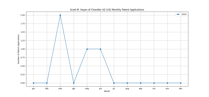
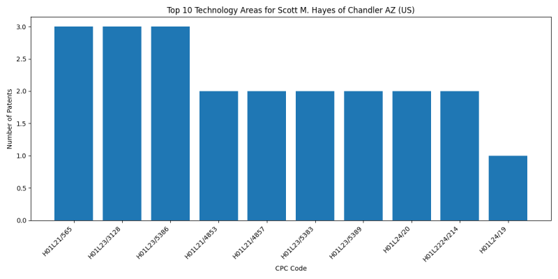
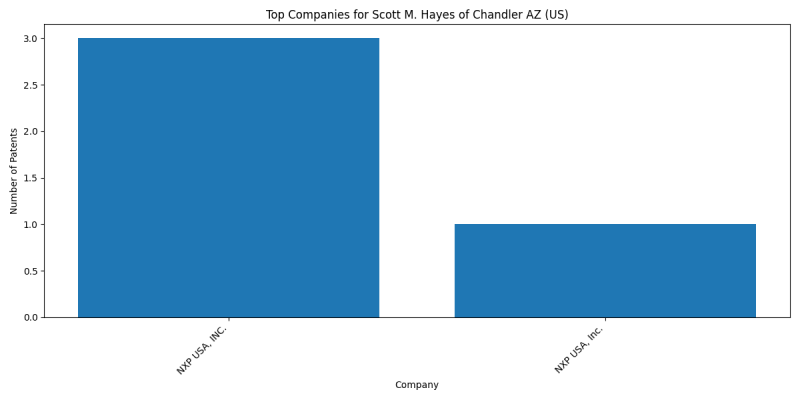
Scott M. Hayes of Chandler AZ (US) is an inventor who has filed 4 patents. Their primary areas of innovation include SEMICONDUCTOR DEVICES NOT COVERED BY CLASS (3 patents), SEMICONDUCTOR DEVICES NOT COVERED BY CLASS (3 patents), the interconnection structure between a plurality of semiconductor chips being formed on, or in, insulating substrates ({ (3 patents), and they have worked with companies such as NXP USA, INC. (3 patents), NXP USA, Inc. (1 patents). Their most frequent collaborators include (3 collaborations), (2 collaborations), (2 collaborations).
Patent Filing Activity
Technology Areas
List of Technology Areas
- H01L21/565 (SEMICONDUCTOR DEVICES NOT COVERED BY CLASS): 3 patents
- H01L23/3128 (SEMICONDUCTOR DEVICES NOT COVERED BY CLASS): 3 patents
- H01L23/5386 (the interconnection structure between a plurality of semiconductor chips being formed on, or in, insulating substrates ({): 3 patents
- H01L21/4853 (Manufacture or treatment of parts, e.g. containers, prior to assembly of the devices, using processes not provided for in a single one of the subgroups): 2 patents
- H01L21/4857 (Manufacture or treatment of parts, e.g. containers, prior to assembly of the devices, using processes not provided for in a single one of the subgroups): 2 patents
- H01L23/5383 ({Multilayer substrates (): 2 patents
- H01L23/5389 (the interconnection structure between a plurality of semiconductor chips being formed on, or in, insulating substrates ({): 2 patents
- H01L24/20 (SEMICONDUCTOR DEVICES NOT COVERED BY CLASS): 2 patents
- H01L2224/214 (SEMICONDUCTOR DEVICES NOT COVERED BY CLASS): 2 patents
- H01L24/19 (SEMICONDUCTOR DEVICES NOT COVERED BY CLASS): 1 patents
- H01L2924/351 (SEMICONDUCTOR DEVICES NOT COVERED BY CLASS): 1 patents
- H01L25/162 (the devices being of types provided for in two or more different main groups of groups): 1 patents
- H01L21/486 (Manufacture or treatment of parts, e.g. containers, prior to assembly of the devices, using processes not provided for in a single one of the subgroups): 1 patents
- H01L21/566 (SEMICONDUCTOR DEVICES NOT COVERED BY CLASS): 1 patents
- H01L23/49816 (Leads, {i.e. metallisations or lead-frames} on insulating substrates, {e.g. chip carriers (shape of the substrate): 1 patents
- H01L23/49822 ({Multilayer substrates (multilayer metallisation on monolayer substrate): 1 patents
- H01L23/49833 (Leads, {i.e. metallisations or lead-frames} on insulating substrates, {e.g. chip carriers (shape of the substrate): 1 patents
- H01L23/49838 (Leads, {i.e. metallisations or lead-frames} on insulating substrates, {e.g. chip carriers (shape of the substrate): 1 patents
- H01L23/5385 (the interconnection structure between a plurality of semiconductor chips being formed on, or in, insulating substrates ({): 1 patents
- H01L25/165 (the devices being of types provided for in two or more different main groups of groups): 1 patents
- H01L24/16 (SEMICONDUCTOR DEVICES NOT COVERED BY CLASS): 1 patents
- H01L23/49593 (Lead-frames {or other flat leads (): 1 patents
- H01L21/4825 (Manufacture or treatment of parts, e.g. containers, prior to assembly of the devices, using processes not provided for in a single one of the subgroups): 1 patents
- H01L21/4842 (Manufacture or treatment of parts, e.g. containers, prior to assembly of the devices, using processes not provided for in a single one of the subgroups): 1 patents
- H01L23/3107 (SEMICONDUCTOR DEVICES NOT COVERED BY CLASS): 1 patents
- H01L23/49503 (Lead-frames {or other flat leads (): 1 patents
- H01L23/4952 (Lead-frames {or other flat leads (): 1 patents
- H01L23/49555 (Lead-frames {or other flat leads (): 1 patents
- H01L23/66 (SEMICONDUCTOR DEVICES NOT COVERED BY CLASS): 1 patents
- H01L23/552 (Protection against radiation, e.g. light {or electromagnetic waves}): 1 patents
- H01P3/06 (Coaxial lines): 1 patents
- H01P11/005 (Apparatus or processes specially adapted for manufacturing waveguides or resonators, lines, or other devices of the waveguide type): 1 patents
- H01Q1/2283 ({mounted in or on the surface of a semiconductor substrate as a chip-type antenna or integrated with other components into an IC package}): 1 patents
- H01Q9/0407 ({Substantially flat resonant element parallel to ground plane, e.g. patch antenna (dipole): 1 patents
- H01L2223/6622 (SEMICONDUCTOR DEVICES NOT COVERED BY CLASS): 1 patents
- H01L2223/6677 (SEMICONDUCTOR DEVICES NOT COVERED BY CLASS): 1 patents
- H01L2924/3025 (SEMICONDUCTOR DEVICES NOT COVERED BY CLASS): 1 patents
Companies
List of Companies
- NXP USA, INC.: 3 patents
- NXP USA, Inc.: 1 patents
Collaborators
- Michael B. Vincent of Chandler AZ (US) (3 collaborations)
- Antonius Hendrikus Jozef Kamphuis (2 collaborations)
- Zhiwei Gong of Chandler AZ (US) (2 collaborations)
- Leo van Gemert (2 collaborations)
- Wen Hung Huang of Chandler AZ (US) (1 collaborations)
- Chayathorn Saklang (1 collaborations)
- Namrata Kanth of Mesa AZ (US) (1 collaborations)
- Stephen Ryan Hooper of Queen Creek AZ (US) (1 collaborations)
- Wen Hung Huang (1 collaborations)
Subcategories
This category has the following 3 subcategories, out of 3 total.
M
S
Z
Pages in category "Scott M. Hayes of Chandler AZ (US)"
This category contains only the following page.
Categories:
- Michael B. Vincent of Chandler AZ (US)
- Antonius Hendrikus Jozef Kamphuis
- Zhiwei Gong of Chandler AZ (US)
- Leo van Gemert
- Wen Hung Huang of Chandler AZ (US)
- Chayathorn Saklang
- Namrata Kanth of Mesa AZ (US)
- Stephen Ryan Hooper of Queen Creek AZ (US)
- Wen Hung Huang
- Scott M. Hayes of Chandler AZ (US)
- Inventors
- Inventors filing patents with NXP USA, INC.
- Inventors filing patents with NXP USA, Inc.


