Category:Ron Rosenberg of San Francisco CA (US)
Jump to navigation
Jump to search
Contents
Ron Rosenberg of San Francisco CA (US)
Executive Summary
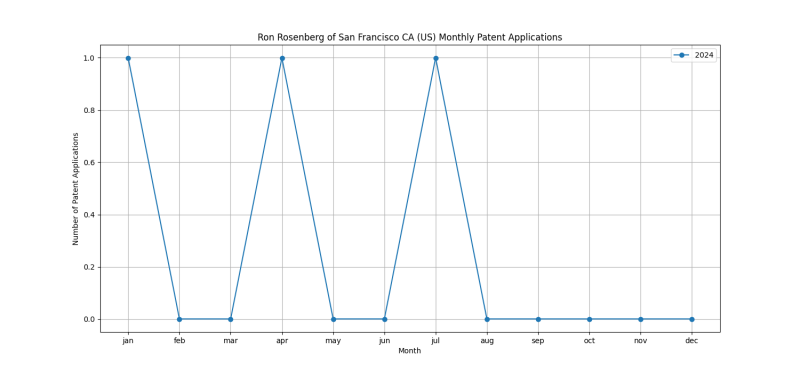
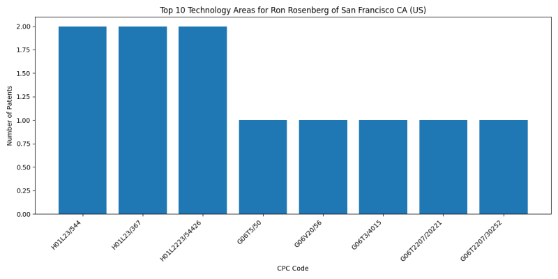
Ron Rosenberg of San Francisco CA (US) is an inventor who has filed 3 patents. Their primary areas of innovation include Marks applied to semiconductor devices {or parts}, e.g. registration marks, {alignment structures, wafer maps (test patterns for characterising or monitoring manufacturing processes (2 patents), Cooling facilitated by shape of device {( (2 patents), SEMICONDUCTOR DEVICES NOT COVERED BY CLASS (2 patents), and they have worked with companies such as Tesla, Inc. (3 patents). Their most frequent collaborators include (2 collaborations), (2 collaborations), (2 collaborations).
Patent Filing Activity
Technology Areas
List of Technology Areas
- H01L23/544 (Marks applied to semiconductor devices {or parts}, e.g. registration marks, {alignment structures, wafer maps (test patterns for characterising or monitoring manufacturing processes): 2 patents
- H01L23/367 (Cooling facilitated by shape of device {(): 2 patents
- H01L2223/54426 (SEMICONDUCTOR DEVICES NOT COVERED BY CLASS): 2 patents
- G06T5/50 (using two or more images, e.g. averaging or subtraction): 1 patents
- G06V20/56 (IMAGE OR VIDEO RECOGNITION OR UNDERSTANDING): 1 patents
- G06T3/4015 (Image demosaicing, e.g. colour filter arrays [CFA] or Bayer patterns): 1 patents
- G06T2207/20221 (Special algorithmic details): 1 patents
- G06T2207/30252 (Subject of image; Context of image processing): 1 patents
Companies
List of Companies
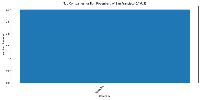
- Tesla, Inc.: 3 patents
Collaborators
- Yong guo Li of Gilroy CA (US) (2 collaborations)
- Rishabh Bhandari of San Carlos CA (US) (2 collaborations)
- Aydin Nabovati (2 collaborations)
- Vijaykumar Krithivasan of Mountain View CA (US) (2 collaborations)
- Mitchell Heschke of Los Altos CA (US) (2 collaborations)
- Matthew Oswald of Austin TX (US) (1 collaborations)
Subcategories
This category has the following 6 subcategories, out of 6 total.
A
M
R
V
Y
Pages in category "Ron Rosenberg of San Francisco CA (US)"
The following 9 pages are in this category, out of 9 total.


