Category:Kyung Suk Oh of Cupertino CA (US)
Jump to navigation
Jump to search
Contents
Kyung Suk Oh of Cupertino CA (US)
Executive Summary
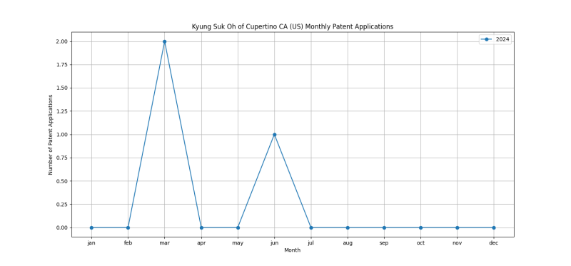
Kyung Suk Oh of Cupertino CA (US) is an inventor who has filed 3 patents. Their primary areas of innovation include STATIC STORES (semiconductor memory devices (2 patents), Supports for storage elements {, e.g. memory modules}; Mounting or fixing of storage elements on such supports (2 patents), Read-write [R-W] timing or clocking circuits; Read-write [R-W] control signal generators or management (1 patents), and they have worked with companies such as Rambus Inc. (3 patents). Their most frequent collaborators include (2 collaborations), (1 collaborations), (1 collaborations).
Patent Filing Activity
Technology Areas
List of Technology Areas
- G11C5/063 (STATIC STORES (semiconductor memory devices): 2 patents
- G11C5/04 (Supports for storage elements {, e.g. memory modules}; Mounting or fixing of storage elements on such supports): 2 patents
- G11C7/22 (Read-write [R-W] timing or clocking circuits; Read-write [R-W] control signal generators or management): 1 patents
- G11C11/4063 (STATIC STORES (semiconductor memory devices): 1 patents
- G11C29/02 (STATIC STORES (semiconductor memory devices): 1 patents
- G11C29/022 (STATIC STORES (semiconductor memory devices): 1 patents
- G11C29/025 (STATIC STORES (semiconductor memory devices): 1 patents
- G11C29/028 (STATIC STORES (semiconductor memory devices): 1 patents
- H05K1/0216 ({Reduction of cross-talk, noise or electromagnetic interference (grounding): 1 patents
- H01B5/02 (CABLES; CONDUCTORS; INSULATORS; SELECTION OF MATERIALS FOR THEIR CONDUCTIVE, INSULATING OR DIELECTRIC PROPERTIES (selection for magnetic properties): 1 patents
- H01L23/49811 ({Additional leads joined to the metallisation on the insulating substrate, e.g. pins, bumps, wires, flat leads (): 1 patents
- H01L23/49838 (Leads, {i.e. metallisations or lead-frames} on insulating substrates, {e.g. chip carriers (shape of the substrate): 1 patents
- H01L23/5286 ({Geometry or} layout of the interconnection structure {(): 1 patents
- H01L23/5223 (SEMICONDUCTOR DEVICES NOT COVERED BY CLASS): 1 patents
- H01L2924/0002 (SEMICONDUCTOR DEVICES NOT COVERED BY CLASS): 1 patents
- G11C8/12 (STATIC STORES (semiconductor memory devices): 1 patents
- G11C5/02 (STATIC STORES (semiconductor memory devices): 1 patents
- G11C5/06 (STATIC STORES (semiconductor memory devices): 1 patents
- G11C7/1012 (Input/output [I/O] data interface arrangements, e.g. I/O data control circuits, I/O data buffers): 1 patents
- G11C7/1045 ({Read-write mode select circuits}): 1 patents
- G11C8/18 (Address timing or clocking circuits; Address control signal generation or management, e.g. for row address strobe [RAS] or column address strobe [CAS] signals): 1 patents
- H01L24/49 (SEMICONDUCTOR DEVICES NOT COVERED BY CLASS): 1 patents
- H01L25/0657 (SEMICONDUCTOR DEVICES NOT COVERED BY CLASS): 1 patents
- H01L24/32 (SEMICONDUCTOR DEVICES NOT COVERED BY CLASS): 1 patents
- H01L24/48 (SEMICONDUCTOR DEVICES NOT COVERED BY CLASS): 1 patents
- H01L24/73 (SEMICONDUCTOR DEVICES NOT COVERED BY CLASS): 1 patents
- H01L2224/16225 (SEMICONDUCTOR DEVICES NOT COVERED BY CLASS): 1 patents
- H01L2224/32145 (SEMICONDUCTOR DEVICES NOT COVERED BY CLASS): 1 patents
- H01L2224/32225 (SEMICONDUCTOR DEVICES NOT COVERED BY CLASS): 1 patents
- H01L2224/45099 (SEMICONDUCTOR DEVICES NOT COVERED BY CLASS): 1 patents
- H01L2224/48095 (SEMICONDUCTOR DEVICES NOT COVERED BY CLASS): 1 patents
- H01L2224/48227 (SEMICONDUCTOR DEVICES NOT COVERED BY CLASS): 1 patents
- H01L2224/48471 (SEMICONDUCTOR DEVICES NOT COVERED BY CLASS): 1 patents
- H01L2224/49171 (SEMICONDUCTOR DEVICES NOT COVERED BY CLASS): 1 patents
- H01L2224/49433 (SEMICONDUCTOR DEVICES NOT COVERED BY CLASS): 1 patents
- H01L2224/73265 (SEMICONDUCTOR DEVICES NOT COVERED BY CLASS): 1 patents
- H01L2225/0651 (SEMICONDUCTOR DEVICES NOT COVERED BY CLASS): 1 patents
- H01L2924/00012 (SEMICONDUCTOR DEVICES NOT COVERED BY CLASS): 1 patents
- H01L2924/00014 (SEMICONDUCTOR DEVICES NOT COVERED BY CLASS): 1 patents
- H01L2924/15311 (SEMICONDUCTOR DEVICES NOT COVERED BY CLASS): 1 patents
- H01L2924/181 (SEMICONDUCTOR DEVICES NOT COVERED BY CLASS): 1 patents
Companies
List of Companies
- Rambus Inc.: 3 patents
Collaborators
- Ian Shaeffer of Los Gatos CA (US) (2 collaborations)
- Ralf M. Schmitt of San Jose CA (US) (1 collaborations)
- Yijong Feng of Los Altos CA (US) (1 collaborations)
- Lawrence Lai of San Jose CA (US) (1 collaborations)
- Fan Ho of San Ramon CA (US) (1 collaborations)
- David A. Secker of San Jose CA (US) (1 collaborations)
- Wayne S. Richardson of Saratoga CA (US) (1 collaborations)
- Akash Bansal of Santa Clara CA (US) (1 collaborations)
- Brian S. Leibowitz of San Francisco CA (US) (1 collaborations)
Subcategories
This category has the following 3 subcategories, out of 3 total.
D
I
K
Categories:
- Ian Shaeffer of Los Gatos CA (US)
- Ralf M. Schmitt of San Jose CA (US)
- Yijong Feng of Los Altos CA (US)
- Lawrence Lai of San Jose CA (US)
- Fan Ho of San Ramon CA (US)
- David A. Secker of San Jose CA (US)
- Wayne S. Richardson of Saratoga CA (US)
- Akash Bansal of Santa Clara CA (US)
- Brian S. Leibowitz of San Francisco CA (US)
- Kyung Suk Oh of Cupertino CA (US)
- Inventors
- Inventors filing patents with Rambus Inc.


