Category:Kuan-Feng LEE
Jump to navigation
Jump to search
Contents
Kuan-Feng LEE
Executive Summary
Kuan-Feng LEE is an inventor who has filed 17 patents. Their primary areas of innovation include the devices being of types provided for in two or more different main groups of groups (3 patents), SEMICONDUCTOR DEVICES NOT COVERED BY CLASS (3 patents), ORGANIC ELECTRIC SOLID-STATE DEVICES (3 patents), and they have worked with companies such as InnoLux Corporation (17 patents). Their most frequent collaborators include (8 collaborations), (7 collaborations), (5 collaborations).
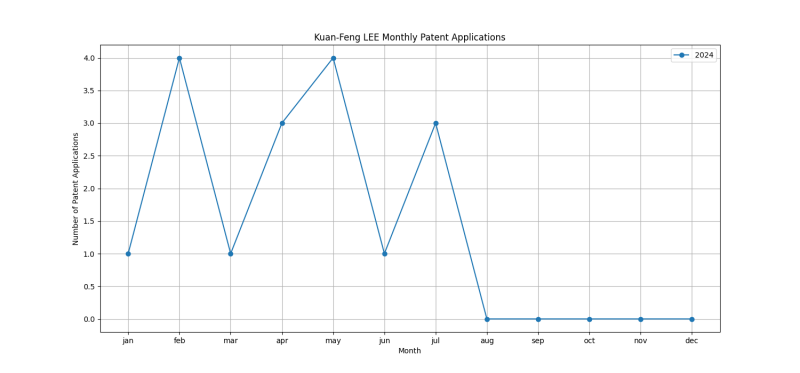
Patent Filing Activity
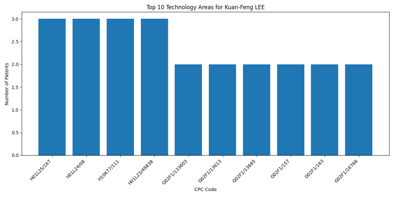
Technology Areas
List of Technology Areas
- H01L25/167 (the devices being of types provided for in two or more different main groups of groups): 3 patents
- H01L24/08 (SEMICONDUCTOR DEVICES NOT COVERED BY CLASS): 3 patents
- H10K77/111 (ORGANIC ELECTRIC SOLID-STATE DEVICES): 3 patents
- H01L23/49838 (Leads, {i.e. metallisations or lead-frames} on insulating substrates, {e.g. chip carriers (shape of the substrate): 3 patents
- G02F1/133603 ({Illuminating devices}): 2 patents
- G02F1/13613 (based on liquid crystals, e.g. single liquid crystal display cells): 2 patents
- G02F1/13685 (based on liquid crystals, e.g. single liquid crystal display cells): 2 patents
- G02F1/157 (based on an electrochromic effect): 2 patents
- G02F1/163 (OPTICAL DEVICES OR ARRANGEMENTS FOR THE CONTROL OF LIGHT BY MODIFICATION OF THE OPTICAL PROPERTIES OF THE MEDIA OF THE ELEMENTS INVOLVED THEREIN; NON-LINEAR OPTICS; FREQUENCY-CHANGING OF LIGHT; OPTICAL LOGIC ELEMENTS; OPTICAL ANALOGUE/DIGITAL CONVERTERS): 2 patents
- G02F1/16766 (by electrophoresis): 2 patents
- G02F1/1677 (by electrophoresis): 2 patents
- H01L27/1225 (the substrate being other than a semiconductor body, e.g. an insulating body): 2 patents
- H01L25/0753 (the devices being of a type provided for in group): 2 patents
- H01L27/156 (including semiconductor components having potential barriers, specially adapted for light emission): 2 patents
- H01L33/62 (Arrangements for conducting electric current to or from the semiconductor body, e.g. lead-frames, wire-bonds or solder balls): 2 patents
- H01L23/5386 (the interconnection structure between a plurality of semiconductor chips being formed on, or in, insulating substrates ({): 2 patents
- H01L2924/182 (SEMICONDUCTOR DEVICES NOT COVERED BY CLASS): 2 patents
- G06F3/0412 ({Digitisers structurally integrated in a display}): 2 patents
- G06F3/044 (by capacitive means): 2 patents
- H01L24/16 (SEMICONDUCTOR DEVICES NOT COVERED BY CLASS): 2 patents
- H01L2224/16227 (SEMICONDUCTOR DEVICES NOT COVERED BY CLASS): 2 patents
- G02F1/133514 ({Colour filters}): 2 patents
- G02F1/133305 (Constructional arrangements; Operation of liquid crystal cells; Circuit arrangements (arrangements or circuits for control of liquid crystal elements in a matrix, not structurally associated with these elements): 2 patents
- G09G3/3233 (with pixel circuitry controlling the current through the light-emitting element): 1 patents
- H01L27/1222 (the substrate being other than a semiconductor body, e.g. an insulating body): 1 patents
- H10K59/1213 (ORGANIC ELECTRIC SOLID-STATE DEVICES): 1 patents
- G09G2300/0426 (ARRANGEMENTS OR CIRCUITS FOR CONTROL OF INDICATING DEVICES USING STATIC MEANS TO PRESENT VARIABLE INFORMATION (arrangements for transferring data between digital computers and displays): 1 patents
- G09G2300/043 (ARRANGEMENTS OR CIRCUITS FOR CONTROL OF INDICATING DEVICES USING STATIC MEANS TO PRESENT VARIABLE INFORMATION (arrangements for transferring data between digital computers and displays): 1 patents
- G09G2300/0809 (ARRANGEMENTS OR CIRCUITS FOR CONTROL OF INDICATING DEVICES USING STATIC MEANS TO PRESENT VARIABLE INFORMATION (arrangements for transferring data between digital computers and displays): 1 patents
- G09G2300/0819 (ARRANGEMENTS OR CIRCUITS FOR CONTROL OF INDICATING DEVICES USING STATIC MEANS TO PRESENT VARIABLE INFORMATION (arrangements for transferring data between digital computers and displays): 1 patents
- G09G2300/0842 (ARRANGEMENTS OR CIRCUITS FOR CONTROL OF INDICATING DEVICES USING STATIC MEANS TO PRESENT VARIABLE INFORMATION (arrangements for transferring data between digital computers and displays): 1 patents
- G09G2300/0861 (ARRANGEMENTS OR CIRCUITS FOR CONTROL OF INDICATING DEVICES USING STATIC MEANS TO PRESENT VARIABLE INFORMATION (arrangements for transferring data between digital computers and displays): 1 patents
- G09G2320/0233 (ARRANGEMENTS OR CIRCUITS FOR CONTROL OF INDICATING DEVICES USING STATIC MEANS TO PRESENT VARIABLE INFORMATION (arrangements for transferring data between digital computers and displays): 1 patents
- G09G2320/045 (ARRANGEMENTS OR CIRCUITS FOR CONTROL OF INDICATING DEVICES USING STATIC MEANS TO PRESENT VARIABLE INFORMATION (arrangements for transferring data between digital computers and displays): 1 patents
- G09G2330/021 (ARRANGEMENTS OR CIRCUITS FOR CONTROL OF INDICATING DEVICES USING STATIC MEANS TO PRESENT VARIABLE INFORMATION (arrangements for transferring data between digital computers and displays): 1 patents
- H10K39/601 (ORGANIC ELECTRIC SOLID-STATE DEVICES): 1 patents
- H10K59/60 (ORGANIC ELECTRIC SOLID-STATE DEVICES): 1 patents
- A61B5/0059 ({using light, e.g. diagnosis by transillumination, diascopy, fluorescence (): 1 patents
- H01L33/58 (Optical field-shaping elements): 1 patents
- H01L31/14 (the light source or sources being controlled by the semiconductor device sensitive to radiation, e.g. image converters, image amplifiers or image storage devices): 1 patents
- H01L31/16 (the semiconductor device sensitive to radiation being controlled by the light source or sources): 1 patents
- H01L33/0012 ({p-i-n devices}): 1 patents
- H01L33/005 ({Processes}): 1 patents
- H01L33/0093 ({Wafer bonding; Removal of the growth substrate}): 1 patents
- H01L33/44 (characterised by the coatings, e.g. passivation layer or anti-reflective coating): 1 patents
- H01L33/48 (characterised by the semiconductor body packages): 1 patents
- H01L24/09 (SEMICONDUCTOR DEVICES NOT COVERED BY CLASS): 1 patents
- H01L23/49816 (Leads, {i.e. metallisations or lead-frames} on insulating substrates, {e.g. chip carriers (shape of the substrate): 1 patents
- H01L23/3677 (Cooling facilitated by shape of device {(): 1 patents
- H01L2224/0801 (SEMICONDUCTOR DEVICES NOT COVERED BY CLASS): 1 patents
- H01L2224/08225 (SEMICONDUCTOR DEVICES NOT COVERED BY CLASS): 1 patents
- H01L2224/0903 (SEMICONDUCTOR DEVICES NOT COVERED BY CLASS): 1 patents
- H01L2924/30101 (SEMICONDUCTOR DEVICES NOT COVERED BY CLASS): 1 patents
- B60R11/0229 (for radio sets, television sets, telephones, or the like; Arrangement of controls thereof): 1 patents
- B60J1/2094 (WINDOWS, WINDSCREENS, NON-FIXED ROOFS, DOORS, OR SIMILAR DEVICES FOR VEHICLES; REMOVABLE EXTERNAL PROTECTIVE COVERINGS SPECIALLY ADAPTED FOR VEHICLES (fastening, suspending, closing, or opening of such devices): 1 patents
- B60R11/0264 (for radio sets, television sets, telephones, or the like; Arrangement of controls thereof): 1 patents
- B60R2011/0026 (VEHICLES, VEHICLE FITTINGS, OR VEHICLE PARTS, NOT OTHERWISE PROVIDED FOR): 1 patents
- H01L27/1214 (the substrate being other than a semiconductor body, e.g. an insulating body): 1 patents
- G02F1/133512 (Structural association of cells with optical devices, e.g. polarisers or reflectors): 1 patents
- G02F1/133553 (Structural association of cells with optical devices, e.g. polarisers or reflectors): 1 patents
- G02F1/1368 (based on liquid crystals, e.g. single liquid crystal display cells): 1 patents
- G02F2201/121 (OPTICAL DEVICES OR ARRANGEMENTS FOR THE CONTROL OF LIGHT BY MODIFICATION OF THE OPTICAL PROPERTIES OF THE MEDIA OF THE ELEMENTS INVOLVED THEREIN; NON-LINEAR OPTICS; FREQUENCY-CHANGING OF LIGHT; OPTICAL LOGIC ELEMENTS; OPTICAL ANALOGUE/DIGITAL CONVERTERS): 1 patents
- G02F2201/123 (OPTICAL DEVICES OR ARRANGEMENTS FOR THE CONTROL OF LIGHT BY MODIFICATION OF THE OPTICAL PROPERTIES OF THE MEDIA OF THE ELEMENTS INVOLVED THEREIN; NON-LINEAR OPTICS; FREQUENCY-CHANGING OF LIGHT; OPTICAL LOGIC ELEMENTS; OPTICAL ANALOGUE/DIGITAL CONVERTERS): 1 patents
- H01L21/561 (SEMICONDUCTOR DEVICES NOT COVERED BY CLASS): 1 patents
- H01L23/3128 (SEMICONDUCTOR DEVICES NOT COVERED BY CLASS): 1 patents
- H01L23/49541 (Lead-frames {or other flat leads (): 1 patents
- H01L24/02 ({Bonding areas (on insulating substrates, e.g. chip carriers,): 1 patents
- H01L24/97 (SEMICONDUCTOR DEVICES NOT COVERED BY CLASS): 1 patents
- H01L2224/02331 (SEMICONDUCTOR DEVICES NOT COVERED BY CLASS): 1 patents
- H01L2224/97 (SEMICONDUCTOR DEVICES NOT COVERED BY CLASS): 1 patents
- G06F3/041662 ({Details of scanning methods, e.g. sampling time, grouping of sub areas or time sharing with display driving (Synchronisation with the driving of the display or the backlighting unit to avoid interferences generated internally): 1 patents
- G06F3/041661 ({Details of scanning methods, e.g. sampling time, grouping of sub areas or time sharing with display driving (Synchronisation with the driving of the display or the backlighting unit to avoid interferences generated internally): 1 patents
- H10K59/40 (ORGANIC ELECTRIC SOLID-STATE DEVICES): 1 patents
- H10K2102/311 (ORGANIC ELECTRIC SOLID-STATE DEVICES): 1 patents
- H01L33/54 (having a particular shape): 1 patents
- H01L33/60 (Reflective elements): 1 patents
- H01L24/13 (SEMICONDUCTOR DEVICES NOT COVERED BY CLASS): 1 patents
- H01L2224/13105 (SEMICONDUCTOR DEVICES NOT COVERED BY CLASS): 1 patents
- H01L2224/13111 (SEMICONDUCTOR DEVICES NOT COVERED BY CLASS): 1 patents
- H01L2224/13124 (SEMICONDUCTOR DEVICES NOT COVERED BY CLASS): 1 patents
- H01L2224/13139 (SEMICONDUCTOR DEVICES NOT COVERED BY CLASS): 1 patents
- H01L2224/13144 (SEMICONDUCTOR DEVICES NOT COVERED BY CLASS): 1 patents
- H01L2224/13147 (SEMICONDUCTOR DEVICES NOT COVERED BY CLASS): 1 patents
- H01L2224/13166 (SEMICONDUCTOR DEVICES NOT COVERED BY CLASS): 1 patents
- H01L2924/12041 (SEMICONDUCTOR DEVICES NOT COVERED BY CLASS): 1 patents
- H01L2933/005 (SEMICONDUCTOR DEVICES NOT COVERED BY CLASS): 1 patents
- H01L2933/0066 (SEMICONDUCTOR DEVICES NOT COVERED BY CLASS): 1 patents
- G02F1/133528 ({Polarisers}): 1 patents
- G02F1/1339 (Constructional arrangements; Operation of liquid crystal cells; Circuit arrangements (arrangements or circuits for control of liquid crystal elements in a matrix, not structurally associated with these elements): 1 patents
- H10K59/50 (ORGANIC ELECTRIC SOLID-STATE DEVICES): 1 patents
- G02F1/133548 (Structural association of cells with optical devices, e.g. polarisers or reflectors): 1 patents
- G02F2201/16 (OPTICAL DEVICES OR ARRANGEMENTS FOR THE CONTROL OF LIGHT BY MODIFICATION OF THE OPTICAL PROPERTIES OF THE MEDIA OF THE ELEMENTS INVOLVED THEREIN; NON-LINEAR OPTICS; FREQUENCY-CHANGING OF LIGHT; OPTICAL LOGIC ELEMENTS; OPTICAL ANALOGUE/DIGITAL CONVERTERS): 1 patents
- G02F2201/50 (OPTICAL DEVICES OR ARRANGEMENTS FOR THE CONTROL OF LIGHT BY MODIFICATION OF THE OPTICAL PROPERTIES OF THE MEDIA OF THE ELEMENTS INVOLVED THEREIN; NON-LINEAR OPTICS; FREQUENCY-CHANGING OF LIGHT; OPTICAL LOGIC ELEMENTS; OPTICAL ANALOGUE/DIGITAL CONVERTERS): 1 patents
- G02F2202/28 (OPTICAL DEVICES OR ARRANGEMENTS FOR THE CONTROL OF LIGHT BY MODIFICATION OF THE OPTICAL PROPERTIES OF THE MEDIA OF THE ELEMENTS INVOLVED THEREIN; NON-LINEAR OPTICS; FREQUENCY-CHANGING OF LIGHT; OPTICAL LOGIC ELEMENTS; OPTICAL ANALOGUE/DIGITAL CONVERTERS): 1 patents
- H05K1/115 (PRINTED CIRCUITS; CASINGS OR CONSTRUCTIONAL DETAILS OF ELECTRIC APPARATUS; MANUFACTURE OF ASSEMBLAGES OF ELECTRICAL COMPONENTS): 1 patents
- H05K1/0271 (PRINTED CIRCUITS; CASINGS OR CONSTRUCTIONAL DETAILS OF ELECTRIC APPARATUS; MANUFACTURE OF ASSEMBLAGES OF ELECTRICAL COMPONENTS): 1 patents
- H05K1/0274 ({Optical details, e.g. printed circuits comprising integral optical means (): 1 patents
- H05K3/4038 (PRINTED CIRCUITS; CASINGS OR CONSTRUCTIONAL DETAILS OF ELECTRIC APPARATUS; MANUFACTURE OF ASSEMBLAGES OF ELECTRICAL COMPONENTS): 1 patents
- H05K2201/096 (PRINTED CIRCUITS; CASINGS OR CONSTRUCTIONAL DETAILS OF ELECTRIC APPARATUS; MANUFACTURE OF ASSEMBLAGES OF ELECTRICAL COMPONENTS): 1 patents
- H05K2201/09827 (PRINTED CIRCUITS; CASINGS OR CONSTRUCTIONAL DETAILS OF ELECTRIC APPARATUS; MANUFACTURE OF ASSEMBLAGES OF ELECTRICAL COMPONENTS): 1 patents
- G09G3/3266 (Details of drivers for scan electrodes): 1 patents
- G06F3/04164 ({Connections between sensors and controllers, e.g. routing lines between electrodes and connection pads}): 1 patents
- H01L23/544 (Marks applied to semiconductor devices {or parts}, e.g. registration marks, {alignment structures, wafer maps (test patterns for characterising or monitoring manufacturing processes): 1 patents
- H01L27/124 (the substrate being other than a semiconductor body, e.g. an insulating body): 1 patents
- H01L27/1251 (the substrate being other than a semiconductor body, e.g. an insulating body): 1 patents
- G09G2310/0297 (ARRANGEMENTS OR CIRCUITS FOR CONTROL OF INDICATING DEVICES USING STATIC MEANS TO PRESENT VARIABLE INFORMATION (arrangements for transferring data between digital computers and displays): 1 patents
- H01L2223/54426 (SEMICONDUCTOR DEVICES NOT COVERED BY CLASS): 1 patents
- G02F1/13338 ({Input devices, e.g. touch panels}): 1 patents
- G02F1/136209 (based on liquid crystals, e.g. single liquid crystal display cells): 1 patents
- G02F1/133723 (Constructional arrangements; Operation of liquid crystal cells; Circuit arrangements (arrangements or circuits for control of liquid crystal elements in a matrix, not structurally associated with these elements): 1 patents
- G02F1/136277 (based on liquid crystals, e.g. single liquid crystal display cells): 1 patents
- G02F1/136222 (based on liquid crystals, e.g. single liquid crystal display cells): 1 patents
- H01L23/293 (SEMICONDUCTOR DEVICES NOT COVERED BY CLASS): 1 patents
- H01L24/24 (SEMICONDUCTOR DEVICES NOT COVERED BY CLASS): 1 patents
- H01L24/19 (SEMICONDUCTOR DEVICES NOT COVERED BY CLASS): 1 patents
- H01L23/49833 (Leads, {i.e. metallisations or lead-frames} on insulating substrates, {e.g. chip carriers (shape of the substrate): 1 patents
- H01L21/4857 (Manufacture or treatment of parts, e.g. containers, prior to assembly of the devices, using processes not provided for in a single one of the subgroups): 1 patents
- H01L21/486 (Manufacture or treatment of parts, e.g. containers, prior to assembly of the devices, using processes not provided for in a single one of the subgroups): 1 patents
- H01L21/563 (SEMICONDUCTOR DEVICES NOT COVERED BY CLASS): 1 patents
- H01L21/566 (SEMICONDUCTOR DEVICES NOT COVERED BY CLASS): 1 patents
- H01L23/5383 ({Multilayer substrates (): 1 patents
- H01L23/3142 (SEMICONDUCTOR DEVICES NOT COVERED BY CLASS): 1 patents
- H01L23/3135 (SEMICONDUCTOR DEVICES NOT COVERED BY CLASS): 1 patents
- H01L2924/1811 (SEMICONDUCTOR DEVICES NOT COVERED BY CLASS): 1 patents
- H01L2924/1815 (SEMICONDUCTOR DEVICES NOT COVERED BY CLASS): 1 patents
- H01L2924/18301 (SEMICONDUCTOR DEVICES NOT COVERED BY CLASS): 1 patents
- H01L2224/16237 (SEMICONDUCTOR DEVICES NOT COVERED BY CLASS): 1 patents
- H01L2224/24011 (SEMICONDUCTOR DEVICES NOT COVERED BY CLASS): 1 patents
- H01L2224/24051 (SEMICONDUCTOR DEVICES NOT COVERED BY CLASS): 1 patents
- H01L2224/24101 (SEMICONDUCTOR DEVICES NOT COVERED BY CLASS): 1 patents
- H01L2224/24137 (SEMICONDUCTOR DEVICES NOT COVERED BY CLASS): 1 patents
- H01L23/3121 (SEMICONDUCTOR DEVICES NOT COVERED BY CLASS): 1 patents
- H01L2924/186 (SEMICONDUCTOR DEVICES NOT COVERED BY CLASS): 1 patents
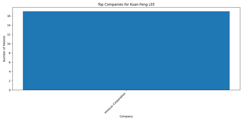
Companies
List of Companies
- InnoLux Corporation: 17 patents
Collaborators
- Tsung-Han TSAI (8 collaborations)
- Yuan-Lin WU (7 collaborations)
- Jia-Yuan CHEN (5 collaborations)
- Yu-Chia HUANG (5 collaborations)
- Jui-Jen YUEH (5 collaborations)
- Chandra LIUS (3 collaborations)
- Chia-Lin YANG (2 collaborations)
- Sheng-Nan CHEN (2 collaborations)
- Chin-Ming HUANG (2 collaborations)
- Cheng-Chi WANG (2 collaborations)
- Lien-Hsiang CHEN (1 collaborations)
- Kung-Chen KUO (1 collaborations)
- Ming-Chun TSENG (1 collaborations)
- Cheng-Hsu CHOU (1 collaborations)
- Kuang-Ming FAN (1 collaborations)
- Li-Wei SUNG (1 collaborations)
- Ker-Yih KAO (1 collaborations)
- Wei-Yuan CHENG (1 collaborations)
Subcategories
This category has the following 7 subcategories, out of 7 total.
C
J
K
T
Y
Categories:
- Tsung-Han TSAI
- Yuan-Lin WU
- Jia-Yuan CHEN
- Yu-Chia HUANG
- Jui-Jen YUEH
- Chandra LIUS
- Chia-Lin YANG
- Sheng-Nan CHEN
- Chin-Ming HUANG
- Cheng-Chi WANG
- Lien-Hsiang CHEN
- Kung-Chen KUO
- Ming-Chun TSENG
- Cheng-Hsu CHOU
- Kuang-Ming FAN
- Li-Wei SUNG
- Ker-Yih KAO
- Wei-Yuan CHENG
- Kuan-Feng LEE
- Inventors
- Inventors filing patents with InnoLux Corporation


