Category:Keitaro TSUCHIYA
Jump to navigation
Jump to search
Contents
Keitaro TSUCHIYA
Executive Summary
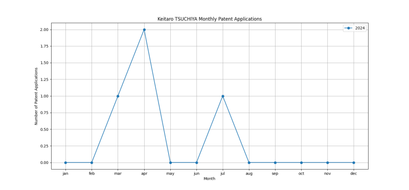
Keitaro TSUCHIYA is an inventor who has filed 4 patents. Their primary areas of innovation include {comprising nitride compounds} (2 patents), {Wafer bonding; Removal of the growth substrate} (2 patents), within the light emitting region, e.g. quantum confinement structure or tunnel barrier (2 patents), and they have worked with companies such as SHIN-ETSU HANDOTAI CO., LTD. (4 patents). Their most frequent collaborators include (2 collaborations), (1 collaborations), (1 collaborations).
Patent Filing Activity
Technology Areas
List of Technology Areas
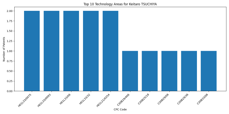
- H01L33/0075 ({comprising nitride compounds}): 2 patents
- H01L33/0093 ({Wafer bonding; Removal of the growth substrate}): 2 patents
- H01L33/06 (within the light emitting region, e.g. quantum confinement structure or tunnel barrier): 2 patents
- H01L33/32 (containing nitrogen): 2 patents
- H01L21/0254 (SEMICONDUCTOR DEVICES NOT COVERED BY CLASS): 2 patents
- C30B29/406 (SINGLE-CRYSTAL GROWTH (by using ultra-high pressure, e.g. for the formation of diamonds,): 1 patents
- C30B25/18 (SINGLE-CRYSTAL GROWTH (by using ultra-high pressure, e.g. for the formation of diamonds,): 1 patents
- C30B29/06 (SINGLE-CRYSTAL GROWTH (by using ultra-high pressure, e.g. for the formation of diamonds,): 1 patents
- C30B29/36 (SINGLE-CRYSTAL GROWTH (by using ultra-high pressure, e.g. for the formation of diamonds,): 1 patents
- C30B33/06 (SINGLE-CRYSTAL GROWTH (by using ultra-high pressure, e.g. for the formation of diamonds,): 1 patents
- H01L21/02389 (SEMICONDUCTOR DEVICES NOT COVERED BY CLASS): 1 patents
- H01L27/1203 ({the substrate comprising an insulating body on a semiconductor body, e.g. SOI (three-dimensional layout): 1 patents
- H01L21/02458 (SEMICONDUCTOR DEVICES NOT COVERED BY CLASS): 1 patents
- H01L21/0262 (SEMICONDUCTOR DEVICES NOT COVERED BY CLASS): 1 patents
- H01L21/7605 (Making of isolation regions between components): 1 patents
- H01L21/76251 (Dielectric regions {, e.g. EPIC dielectric isolation, LOCOS; Trench refilling techniques, SOI technology, use of channel stoppers}): 1 patents
- H01L29/2003 (SEMICONDUCTOR DEVICES NOT COVERED BY CLASS): 1 patents
Companies
List of Companies
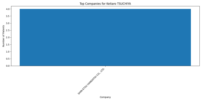
- SHIN-ETSU HANDOTAI CO., LTD.: 4 patents
Collaborators
- Masato YAMADA (2 collaborations)
- Weifeng QU (1 collaborations)
- Yoshihiro KUBOTA (1 collaborations)
- Kazutoshi NAGATA (1 collaborations)
- Ippei KUBONO (1 collaborations)
- Kazunori HAGIMOTO (1 collaborations)
- Masaru SHINOMIYA (1 collaborations)
Subcategories
This category has the following 6 subcategories, out of 6 total.


