Category:Hiroumi KINJO
Jump to navigation
Jump to search
Contents
Hiroumi KINJO
Executive Summary
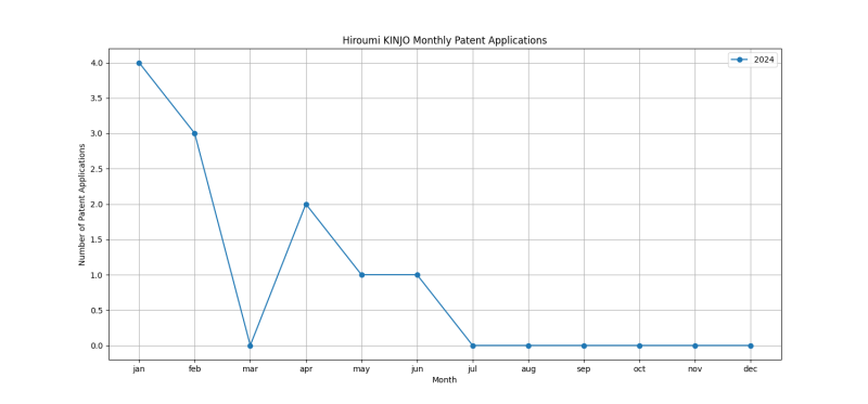
Hiroumi KINJO is an inventor who has filed 11 patents. Their primary areas of innovation include ORGANIC ELECTRIC SOLID-STATE DEVICES (3 patents), ORGANIC ELECTRIC SOLID-STATE DEVICES (2 patents), {Connections between sensors and controllers, e.g. routing lines between electrodes and connection pads} (1 patents), and they have worked with companies such as Japan Display Inc. (11 patents). Their most frequent collaborators include (5 collaborations), (4 collaborations), (3 collaborations).
Patent Filing Activity
Technology Areas
List of Technology Areas
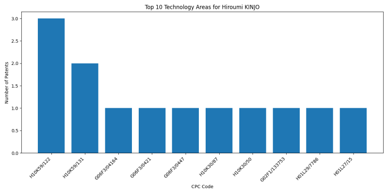
- H10K59/122 (ORGANIC ELECTRIC SOLID-STATE DEVICES): 3 patents
- H10K59/131 (ORGANIC ELECTRIC SOLID-STATE DEVICES): 2 patents
- G06F3/04164 ({Connections between sensors and controllers, e.g. routing lines between electrodes and connection pads}): 1 patents
- G06F3/0421 ({by interrupting or reflecting a light beam, e.g. optical touch-screen}): 1 patents
- G06F3/0447 ({Position sensing using the local deformation of sensor cells}): 1 patents
- H10K30/87 (ORGANIC ELECTRIC SOLID-STATE DEVICES): 1 patents
- H10K30/50 (ORGANIC ELECTRIC SOLID-STATE DEVICES): 1 patents
- G02F1/133753 (Constructional arrangements; Operation of liquid crystal cells; Circuit arrangements (arrangements or circuits for control of liquid crystal elements in a matrix, not structurally associated with these elements): 1 patents
- H01L29/7786 (SEMICONDUCTOR DEVICES NOT COVERED BY CLASS): 1 patents
- H01L27/15 (including semiconductor components having potential barriers, specially adapted for light emission): 1 patents
- H01L29/2003 (SEMICONDUCTOR DEVICES NOT COVERED BY CLASS): 1 patents
- H01L33/32 (containing nitrogen): 1 patents
- H01L33/58 (Optical field-shaping elements): 1 patents
- G06F1/1652 ({the display being flexible, e.g. mimicking a sheet of paper, or rollable}): 1 patents
- G06F1/1681 ({Details related solely to hinges (hinge details related to the transmission of signals or power are classified in): 1 patents
- H10K59/1201 (ORGANIC ELECTRIC SOLID-STATE DEVICES): 1 patents
- G02F1/13718 (based on liquid crystals, e.g. single liquid crystal display cells): 1 patents
- G02F1/133761 (Constructional arrangements; Operation of liquid crystal cells; Circuit arrangements (arrangements or circuits for control of liquid crystal elements in a matrix, not structurally associated with these elements): 1 patents
- G02F1/133788 (Constructional arrangements; Operation of liquid crystal cells; Circuit arrangements (arrangements or circuits for control of liquid crystal elements in a matrix, not structurally associated with these elements): 1 patents
- G02F1/133757 (Constructional arrangements; Operation of liquid crystal cells; Circuit arrangements (arrangements or circuits for control of liquid crystal elements in a matrix, not structurally associated with these elements): 1 patents
- G02F1/133365 ({Cells in which the active layer comprises a liquid crystalline polymer}): 1 patents
- G02F1/133536 (Structural association of cells with optical devices, e.g. polarisers or reflectors): 1 patents
- H10K50/19 (ORGANIC ELECTRIC SOLID-STATE DEVICES): 1 patents
- H10K71/00 (Manufacture or treatment specially adapted for the organic devices covered by this subclass): 1 patents
- H10K50/156 (ORGANIC ELECTRIC SOLID-STATE DEVICES): 1 patents
- H10K50/181 (ORGANIC ELECTRIC SOLID-STATE DEVICES): 1 patents
- H10K50/171 (ORGANIC ELECTRIC SOLID-STATE DEVICES): 1 patents
- H10K59/353 (ORGANIC ELECTRIC SOLID-STATE DEVICES): 1 patents
- H05K1/0283 (PRINTED CIRCUITS; CASINGS OR CONSTRUCTIONAL DETAILS OF ELECTRIC APPARATUS; MANUFACTURE OF ASSEMBLAGES OF ELECTRICAL COMPONENTS): 1 patents
- H05K2201/10151 (PRINTED CIRCUITS; CASINGS OR CONSTRUCTIONAL DETAILS OF ELECTRIC APPARATUS; MANUFACTURE OF ASSEMBLAGES OF ELECTRICAL COMPONENTS): 1 patents
- H10K50/814 (ORGANIC ELECTRIC SOLID-STATE DEVICES): 1 patents
- H10K59/123 (ORGANIC ELECTRIC SOLID-STATE DEVICES): 1 patents
- H01L33/325 ({characterised by the doping materials}): 1 patents
- C23C14/0641 (COATING METALLIC MATERIAL; COATING MATERIAL WITH METALLIC MATERIAL; SURFACE TREATMENT OF METALLIC MATERIAL BY DIFFUSION INTO THE SURFACE, BY CHEMICAL CONVERSION OR SUBSTITUTION; COATING BY VACUUM EVAPORATION, BY SPUTTERING, BY ION IMPLANTATION OR BY CHEMICAL VAPOUR DEPOSITION, IN GENERAL (making metal-coated products by extrusion): 1 patents
- H01L33/22 (Roughened surfaces, e.g. at the interface between epitaxial layers): 1 patents
Companies
List of Companies
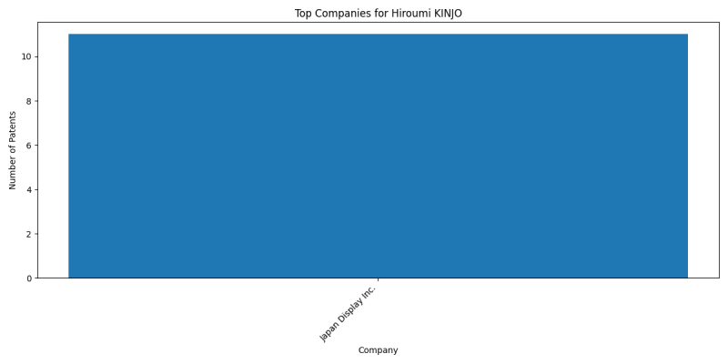
- Japan Display Inc.: 11 patents
Collaborators
- Hayata AOKI (5 collaborations)
- Masumi NISHIMURA (4 collaborations)
- Masatomo HISHINUMA (3 collaborations)
- Shinichiro OKA (3 collaborations)
- Koichi IGETA (2 collaborations)
- Yasuyuki YAMADA (1 collaborations)
- Takahiro USHIKUBO (1 collaborations)
- Jun NITTA (1 collaborations)
- Yosuke HYODO (1 collaborations)
- Takumi SANO (1 collaborations)
Subcategories
This category has the following 4 subcategories, out of 4 total.


