Category:Durai Vishak Nirmal Ramaswamy of Boise ID (US)
Jump to navigation
Jump to search
Contents
Durai Vishak Nirmal Ramaswamy of Boise ID (US)
Executive Summary
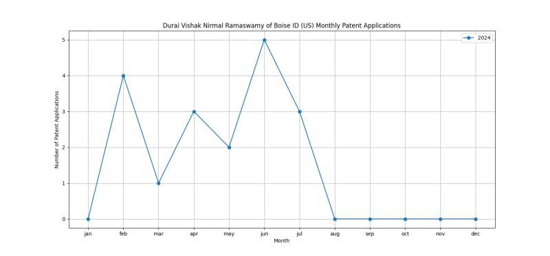
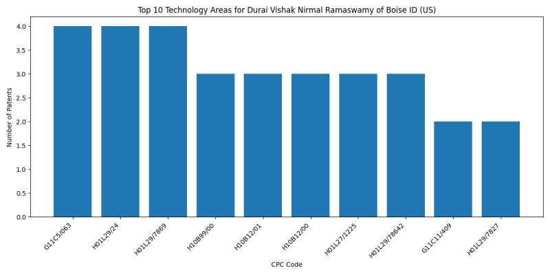
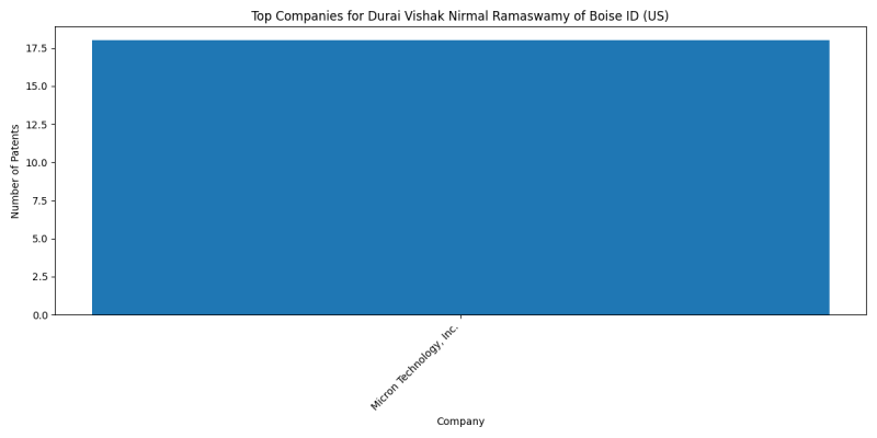
Durai Vishak Nirmal Ramaswamy of Boise ID (US) is an inventor who has filed 18 patents. Their primary areas of innovation include STATIC STORES (semiconductor memory devices (4 patents), SEMICONDUCTOR DEVICES NOT COVERED BY CLASS (4 patents), SEMICONDUCTOR DEVICES NOT COVERED BY CLASS (4 patents), and they have worked with companies such as Micron Technology, Inc. (18 patents). Their most frequent collaborators include (14 collaborations), (11 collaborations), (9 collaborations).
Patent Filing Activity
Technology Areas
List of Technology Areas
- G11C5/063 (STATIC STORES (semiconductor memory devices): 4 patents
- H01L29/24 (SEMICONDUCTOR DEVICES NOT COVERED BY CLASS): 4 patents
- H01L29/7869 (SEMICONDUCTOR DEVICES NOT COVERED BY CLASS): 4 patents
- H10B99/00 (ELECTRONIC MEMORY DEVICES): 3 patents
- H10B12/01 (ELECTRONIC MEMORY DEVICES): 3 patents
- H10B12/00 (Dynamic random access memory [DRAM] devices): 3 patents
- H01L27/1225 (the substrate being other than a semiconductor body, e.g. an insulating body): 3 patents
- H01L29/78642 (SEMICONDUCTOR DEVICES NOT COVERED BY CLASS): 3 patents
- G11C11/409 (STATIC STORES (semiconductor memory devices): 2 patents
- H01L29/7827 (SEMICONDUCTOR DEVICES NOT COVERED BY CLASS): 2 patents
- H10B12/20 (ELECTRONIC MEMORY DEVICES): 2 patents
- G11C11/405 (with three charge-transfer gates, e.g. MOS transistors, per cell): 2 patents
- G11C11/4096 (Input/output [I/O] data management or control circuits, e.g. reading or writing circuits, I/O drivers or bit-line switches): 2 patents
- H10B51/20 (ELECTRONIC MEMORY DEVICES): 2 patents
- H10B51/10 (ELECTRONIC MEMORY DEVICES): 2 patents
- H10B53/10 (ELECTRONIC MEMORY DEVICES): 2 patents
- H01L27/124 (the substrate being other than a semiconductor body, e.g. an insulating body): 2 patents
- H10B63/34 (ELECTRONIC MEMORY DEVICES): 2 patents
- H10N70/883 (No explanation available): 2 patents
- H01L29/66969 ({of devices having semiconductor bodies not comprising group 14 or group 13/15 materials (comprising selenium or tellurium in uncombined form other than as impurities in semiconductor bodies of other materials, comprising cuprous oxide or cuprous iodide): 2 patents
- H10B12/50 (ELECTRONIC MEMORY DEVICES): 2 patents
- G11C11/4023 (STATIC STORES (semiconductor memory devices): 1 patents
- H01L29/22 (SEMICONDUCTOR DEVICES NOT COVERED BY CLASS): 1 patents
- G11C11/2257 ({Word-line or row circuits}): 1 patents
- G11C7/067 (Sense amplifiers; Associated circuits {, e.g. timing or triggering circuits}): 1 patents
- G11C11/2297 ({Power supply circuits}): 1 patents
- H10B43/50 (ELECTRONIC MEMORY DEVICES): 1 patents
- H01L29/1062 (SEMICONDUCTOR DEVICES NOT COVERED BY CLASS): 1 patents
- H01L29/42396 (SEMICONDUCTOR DEVICES NOT COVERED BY CLASS): 1 patents
- H10B41/10 (ELECTRONIC MEMORY DEVICES): 1 patents
- H10B41/20 (ELECTRONIC MEMORY DEVICES): 1 patents
- H10B53/20 (ELECTRONIC MEMORY DEVICES): 1 patents
- H01L29/40111 (SEMICONDUCTOR DEVICES NOT COVERED BY CLASS): 1 patents
- H01L29/516 (SEMICONDUCTOR DEVICES NOT COVERED BY CLASS): 1 patents
- H01L29/6684 (SEMICONDUCTOR DEVICES NOT COVERED BY CLASS): 1 patents
- H01L29/78391 (SEMICONDUCTOR DEVICES NOT COVERED BY CLASS): 1 patents
- H01L27/1251 (the substrate being other than a semiconductor body, e.g. an insulating body): 1 patents
- H01L29/78672 (SEMICONDUCTOR DEVICES NOT COVERED BY CLASS): 1 patents
- H01L29/7881 (SEMICONDUCTOR DEVICES NOT COVERED BY CLASS): 1 patents
- H10B53/50 (ELECTRONIC MEMORY DEVICES): 1 patents
- G11C11/221 ({using ferroelectric capacitors}): 1 patents
- H10B53/30 (ELECTRONIC MEMORY DEVICES): 1 patents
- H10B53/40 (ELECTRONIC MEMORY DEVICES): 1 patents
- H10B41/27 (ELECTRONIC MEMORY DEVICES): 1 patents
- G11C5/025 ({Geometric lay-out considerations of storage- and peripheral-blocks in a semiconductor storage device (geometrical lay-out of the components in integrated circuits,): 1 patents
- G11C5/06 (STATIC STORES (semiconductor memory devices): 1 patents
- H10B43/27 (ELECTRONIC MEMORY DEVICES): 1 patents
- H10B63/84 (ELECTRONIC MEMORY DEVICES): 1 patents
- G11C5/12 (STATIC STORES (semiconductor memory devices): 1 patents
- G11C13/0002 ({using resistive RAM [RRAM] elements}): 1 patents
- H01L21/823487 ({with a particular manufacturing method of vertical transistor structures, i.e. with channel vertical to the substrate surface (with a current flow parallel to the substrate surface): 1 patents
- H01L29/4908 (SEMICONDUCTOR DEVICES NOT COVERED BY CLASS): 1 patents
- H01L29/66666 (SEMICONDUCTOR DEVICES NOT COVERED BY CLASS): 1 patents
- H01L29/66795 (SEMICONDUCTOR DEVICES NOT COVERED BY CLASS): 1 patents
- H01L29/78696 (SEMICONDUCTOR DEVICES NOT COVERED BY CLASS): 1 patents
- H10B63/22 (ELECTRONIC MEMORY DEVICES): 1 patents
- H10B63/24 (ELECTRONIC MEMORY DEVICES): 1 patents
- H10N70/011 (No explanation available): 1 patents
- H10N70/245 (No explanation available): 1 patents
- H10N70/828 (No explanation available): 1 patents
- H10N70/841 (No explanation available): 1 patents
- G11C11/401 (forming cells needing refreshing or charge regeneration, i.e. dynamic cells): 1 patents
- G11C2213/79 (STATIC STORES (semiconductor memory devices): 1 patents
- H10B63/10 (ELECTRONIC MEMORY DEVICES): 1 patents
- H10B63/845 (ELECTRONIC MEMORY DEVICES): 1 patents
- H01L27/092 (SEMICONDUCTOR DEVICES NOT COVERED BY CLASS): 1 patents
- H01L27/1207 ({combined with devices in contact with the semiconductor body, i.e. bulk/SOI hybrid circuits}): 1 patents
- H01L27/1255 (the substrate being other than a semiconductor body, e.g. an insulating body): 1 patents
- H01L27/1259 (the substrate being other than a semiconductor body, e.g. an insulating body): 1 patents
- H01L29/267 (SEMICONDUCTOR DEVICES NOT COVERED BY CLASS): 1 patents
- H01L29/42392 (SEMICONDUCTOR DEVICES NOT COVERED BY CLASS): 1 patents
- G11C11/4097 (Bit-line organisation, e.g. bit-line layout, folded bit lines): 1 patents
- G11C11/408 (Address circuits): 1 patents
- G11C11/4091 (Sense or sense/refresh amplifiers, or associated sense circuitry, e.g. for coupled bit-line precharging, equalising or isolating): 1 patents
- G11C11/4093 (Input/output [I/O] data interface arrangements, e.g. data buffers): 1 patents
- H01L29/42384 (SEMICONDUCTOR DEVICES NOT COVERED BY CLASS): 1 patents
- H10B12/05 (ELECTRONIC MEMORY DEVICES): 1 patents
- H10B12/30 (ELECTRONIC MEMORY DEVICES): 1 patents
- H01L23/5286 ({Geometry or} layout of the interconnection structure {(): 1 patents
Companies
List of Companies
- Micron Technology, Inc.: 18 patents
Collaborators
- Kamal M. Karda of Boise ID (US) (14 collaborations)
- Haitao Liu of Boise ID (US) (11 collaborations)
- Karthik Sarpatwari of Boise ID (US) (9 collaborations)
- Giorgio Servalli (2 collaborations)
- Marcello Mariani (2 collaborations)
- Alessandro Calderoni of Boise ID (US) (2 collaborations)
- Angelo Visconti (1 collaborations)
- Eric S. Carman of San Francisco CA (US) (1 collaborations)
- Richard E. Fackenthal of Carmichael CA (US) (1 collaborations)
- Kamal Karda of Boise ID (US) (1 collaborations)
- Yunfei Gao of Boise ID (US) (1 collaborations)
- Sanh D. Tang of Meridian ID (US) (1 collaborations)
- Deepak Chandra Pandey (1 collaborations)
- Pankaj Sharma of Boise ID (US) (1 collaborations)
- Chandra Mouli of Boise ID (US) (1 collaborations)
- Yi Fang Lee of Boise ID (US) (1 collaborations)
- Ramanathan Gandhi of Boise ID (US) (1 collaborations)
- Scott E. Sills of Boise ID (US) (1 collaborations)
- Sameer Chhajed of Boise ID (US) (1 collaborations)
- Srinivas Pulugurtha of Boise ID (US) (1 collaborations)
- Kirk D. Prall of Boise ID (US) (1 collaborations)
Subcategories
This category has the following 3 subcategories, out of 3 total.
D
H
K
Pages in category "Durai Vishak Nirmal Ramaswamy of Boise ID (US)"
The following 28 pages are in this category, out of 28 total.
1
- 18204773. FORMATION FOR MEMORY CELLS simplified abstract (Micron Technology, Inc.)
- 18238269. MEMORY DEVICE HAVING 2-TRANSISTOR VERTICAL MEMORY CELL AND SEPARATE READ AND WRITE DATA LINES simplified abstract (Micron Technology, Inc.)
- 18238291. MEMORY DEVICE HAVING 2-TRANSISTOR VERTICAL MEMORY CELL AND MEMORY ELEMENT BETWEEN CHANNEL REGION AND CONDUCTIVE PLATE simplified abstract (Micron Technology, Inc.)
- 18244069. MEMORY DEVICE HAVING 2-TRANSISTOR VERTICAL MEMORY CELL AND SEPARATE READ AND WRITE GATES simplified abstract (MICRON TECHNOLOGY, INC.)
- 18387921. Integrated Assemblies Comprising Hydrogen Diffused Within Two or More Different Semiconductor Materials, and Methods of Forming Integrated Assemblies simplified abstract (Micron Technology, Inc.)
- 18388769. MEMORY DEVICE HAVING 2-TRANSISTOR VERTICAL MEMORY CELL simplified abstract (Micron Technology, Inc.)
- 18400082. MEMORY DEVICE HAVING 2-TRANSISTOR MEMORY CELL AND ACCESS LINE PLATE simplified abstract (Micron Technology, Inc.)
- 18429677. Integrated Assemblies and Methods of Forming Integrated Assemblies simplified abstract (Micron Technology, Inc.)
- 18510464. MEMORY STRUCTURES WITH VOIDS simplified abstract (Micron Technology, Inc.)
- 18519964. SEMICONDUCTOR DEVICES AND HYBRID TRANSISTORS simplified abstract (Micron Technology, Inc.)
- 18530113. SEMICONDUCTOR DEVICES COMPRISING TRANSISTORS HAVING INCREASED THRESHOLD VOLTAGE AND RELATED METHODS AND SYSTEMS simplified abstract (Micron Technology, Inc.)
- 18615490. MEMORY DEVICE HAVING SHARED READ/WRITE ACCESS LINE FOR 2-TRANSISTOR VERTICAL MEMORY CELL simplified abstract (Micron Technology, Inc.)
- 18623929. MEMORY DEVICE HAVING 2-TRANSISTOR VERTICAL MEMORY CELL AND SHIELD STRUCTURES simplified abstract (Micron Technology, Inc.)
- 18623956. MEMORY DEVICE HAVING 2-TRANSISTOR VERTICAL MEMORY CELL AND WRAPPED DATA LINE STRUCTURE simplified abstract (Micron Technology, Inc.)
- 18818295. MEMORY DEVICE HAVING 2-TRANSISTOR VERTICAL MEMORY CELL AND SHIELD STRUCTURES (Micron Technology, Inc.)
M
- Micron technology, inc. (20240127877). DIFFERENTIAL STORAGE IN MEMORY ARRAYS simplified abstract
- Micron technology, inc. (20240164113). MEMORY STRUCTURES WITH VOIDS simplified abstract
- Micron technology, inc. (20240188273). MEMORY DEVICE HAVING TIERS OF 2-TRANSISTOR MEMORY CELLS simplified abstract
- Micron technology, inc. (20240188274). MEMORY DEVICE HAVING TIERS OF 2-TRANSISTOR MEMORY CELLS AND CHARGE STORAGE STRUCTURE HAVING MULTIPLE PORTIONS simplified abstract
- Micron technology, inc. (20240188302). MEMORY DEVICE INCLUDING TIERS OF FeFET MEMORY CELLS AND VERTICAL CONTROL GATES simplified abstract
- Micron technology, inc. (20240196604). MEMORY DEVICE HAVING 2-TRANSISTOR VERTICAL MEMORY CELL simplified abstract
- Micron technology, inc. (20240233797). MEMORY DEVICE HAVING SHARED READ/WRITE ACCESS LINE FOR 2-TRANSISTOR VERTICAL MEMORY CELL simplified abstract
- Micron technology, inc. (20240251543). MEMORY DEVICE HAVING 2-TRANSISTOR VERTICAL MEMORY CELL AND SHIELD STRUCTURES simplified abstract
- Micron technology, inc. (20240251563). MEMORY DEVICE HAVING 2-TRANSISTOR VERTICAL MEMORY CELL AND WRAPPED DATA LINE STRUCTURE simplified abstract
- Micron technology, inc. (20240265960). Memory Arrays, Ferroelectric Transistors, and Methods of Reading and Writing Relative to Memory Cells of Memory Arrays simplified abstract
- Micron technology, inc. (20240413154). Integrated Assemblies Comprising Hydrogen Diffused Within Two or More Different Semiconductor Materials, and Methods of Forming Integrated Assemblies
- Micron technology, inc. (20240414911). MEMORY DEVICE HAVING SHARED ACCESS LINE FOR 2-TRANSISTOR VERTICAL MEMORY CELL
- Micron technology, inc. (20240420750). MEMORY DEVICE HAVING 2-TRANSISTOR VERTICAL MEMORY CELL AND SHIELD STRUCTURES
Categories:
- Kamal M. Karda of Boise ID (US)
- Haitao Liu of Boise ID (US)
- Karthik Sarpatwari of Boise ID (US)
- Giorgio Servalli
- Marcello Mariani
- Alessandro Calderoni of Boise ID (US)
- Angelo Visconti
- Eric S. Carman of San Francisco CA (US)
- Richard E. Fackenthal of Carmichael CA (US)
- Kamal Karda of Boise ID (US)
- Yunfei Gao of Boise ID (US)
- Sanh D. Tang of Meridian ID (US)
- Deepak Chandra Pandey
- Pankaj Sharma of Boise ID (US)
- Chandra Mouli of Boise ID (US)
- Yi Fang Lee of Boise ID (US)
- Ramanathan Gandhi of Boise ID (US)
- Scott E. Sills of Boise ID (US)
- Sameer Chhajed of Boise ID (US)
- Srinivas Pulugurtha of Boise ID (US)
- Kirk D. Prall of Boise ID (US)
- Durai Vishak Nirmal Ramaswamy of Boise ID (US)
- Inventors
- Inventors filing patents with Micron Technology, Inc.


