Category:Chung-Shi Liu
Jump to navigation
Jump to search
Contents
Chung-Shi Liu
Executive Summary
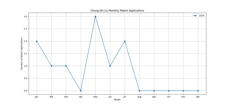
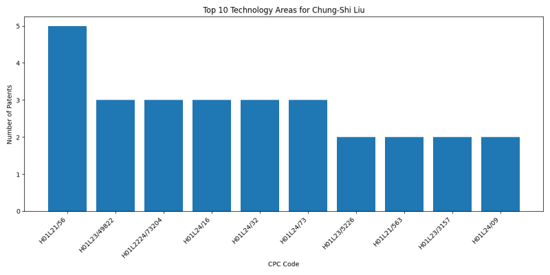
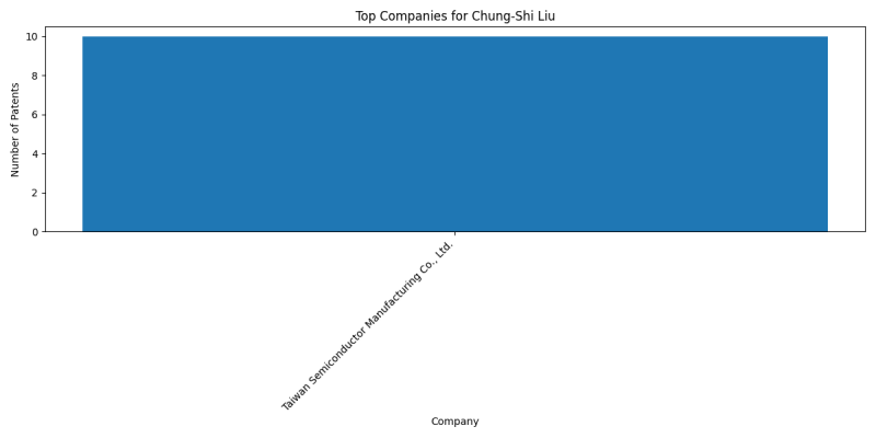
Chung-Shi Liu is an inventor who has filed 10 patents. Their primary areas of innovation include SEMICONDUCTOR DEVICES NOT COVERED BY CLASS (5 patents), {Multilayer substrates (multilayer metallisation on monolayer substrate (3 patents), SEMICONDUCTOR DEVICES NOT COVERED BY CLASS (3 patents), and they have worked with companies such as Taiwan Semiconductor Manufacturing Co., Ltd. (10 patents). Their most frequent collaborators include (6 collaborations), (4 collaborations), (3 collaborations).
Patent Filing Activity
Technology Areas
List of Technology Areas
- H01L21/56 (SEMICONDUCTOR DEVICES NOT COVERED BY CLASS): 5 patents
- H01L23/49822 ({Multilayer substrates (multilayer metallisation on monolayer substrate): 3 patents
- H01L2224/73204 (SEMICONDUCTOR DEVICES NOT COVERED BY CLASS): 3 patents
- H01L24/16 (SEMICONDUCTOR DEVICES NOT COVERED BY CLASS): 3 patents
- H01L24/32 (SEMICONDUCTOR DEVICES NOT COVERED BY CLASS): 3 patents
- H01L24/73 (SEMICONDUCTOR DEVICES NOT COVERED BY CLASS): 3 patents
- H01L23/5226 (SEMICONDUCTOR DEVICES NOT COVERED BY CLASS): 2 patents
- H01L21/563 (SEMICONDUCTOR DEVICES NOT COVERED BY CLASS): 2 patents
- H01L23/3157 ({Partial encapsulation or coating (mask layer used as insulation layer): 2 patents
- H01L24/09 (SEMICONDUCTOR DEVICES NOT COVERED BY CLASS): 2 patents
- H01L24/81 (SEMICONDUCTOR DEVICES NOT COVERED BY CLASS): 2 patents
- H01L23/49816 (Leads, {i.e. metallisations or lead-frames} on insulating substrates, {e.g. chip carriers (shape of the substrate): 2 patents
- H01L24/13 (SEMICONDUCTOR DEVICES NOT COVERED BY CLASS): 2 patents
- H01L2224/13111 (SEMICONDUCTOR DEVICES NOT COVERED BY CLASS): 2 patents
- H01L2224/13147 (SEMICONDUCTOR DEVICES NOT COVERED BY CLASS): 2 patents
- H01L2224/13155 (SEMICONDUCTOR DEVICES NOT COVERED BY CLASS): 2 patents
- H01L2224/16225 (SEMICONDUCTOR DEVICES NOT COVERED BY CLASS): 2 patents
- H01L2224/32225 (SEMICONDUCTOR DEVICES NOT COVERED BY CLASS): 2 patents
- H01L2924/15311 (SEMICONDUCTOR DEVICES NOT COVERED BY CLASS): 2 patents
- H01L23/3114 (SEMICONDUCTOR DEVICES NOT COVERED BY CLASS): 2 patents
- H01L24/17 (SEMICONDUCTOR DEVICES NOT COVERED BY CLASS): 2 patents
- H01L23/3677 (Cooling facilitated by shape of device {(): 2 patents
- H01L23/3128 (SEMICONDUCTOR DEVICES NOT COVERED BY CLASS): 2 patents
- H01L23/3736 ({Metallic materials (): 2 patents
- H01L21/76802 (Applying interconnections to be used for carrying current between separate components within a device {comprising conductors and dielectrics}): 2 patents
- H01L23/31 (SEMICONDUCTOR DEVICES NOT COVERED BY CLASS): 2 patents
- H01L23/49811 ({Additional leads joined to the metallisation on the insulating substrate, e.g. pins, bumps, wires, flat leads (): 2 patents
- H01L21/4853 (Manufacture or treatment of parts, e.g. containers, prior to assembly of the devices, using processes not provided for in a single one of the subgroups): 2 patents
- H01L25/18 (the devices being of types provided for in two or more different subgroups of the same main group of groups): 2 patents
- H01L23/5389 (the interconnection structure between a plurality of semiconductor chips being formed on, or in, insulating substrates ({): 2 patents
- H01L21/566 (SEMICONDUCTOR DEVICES NOT COVERED BY CLASS): 1 patents
- H01L21/6835 ({using temporarily an auxiliary support}): 1 patents
- H01L21/76816 ({Aspects relating to the layout of the pattern or to the size of vias or trenches (layout of the interconnections per se): 1 patents
- H01L2221/68345 (SEMICONDUCTOR DEVICES NOT COVERED BY CLASS): 1 patents
- H01L2221/68359 (SEMICONDUCTOR DEVICES NOT COVERED BY CLASS): 1 patents
- H01L2221/68381 (SEMICONDUCTOR DEVICES NOT COVERED BY CLASS): 1 patents
- H01L2224/02331 (SEMICONDUCTOR DEVICES NOT COVERED BY CLASS): 1 patents
- H01L2224/13101 (SEMICONDUCTOR DEVICES NOT COVERED BY CLASS): 1 patents
- H01L2224/81005 (SEMICONDUCTOR DEVICES NOT COVERED BY CLASS): 1 patents
- H01L2224/81193 (SEMICONDUCTOR DEVICES NOT COVERED BY CLASS): 1 patents
- H01L2224/81801 (SEMICONDUCTOR DEVICES NOT COVERED BY CLASS): 1 patents
- H01L2924/1436 (SEMICONDUCTOR DEVICES NOT COVERED BY CLASS): 1 patents
- H01L2924/18161 (SEMICONDUCTOR DEVICES NOT COVERED BY CLASS): 1 patents
- H01L2224/175 (SEMICONDUCTOR DEVICES NOT COVERED BY CLASS): 1 patents
- H01L2224/81224 (SEMICONDUCTOR DEVICES NOT COVERED BY CLASS): 1 patents
- H01L2924/3511 (SEMICONDUCTOR DEVICES NOT COVERED BY CLASS): 1 patents
- H01L24/33 (SEMICONDUCTOR DEVICES NOT COVERED BY CLASS): 1 patents
- H10B80/00 (Assemblies of multiple devices comprising at least one memory device covered by this subclass): 1 patents
- H01L2224/29124 (SEMICONDUCTOR DEVICES NOT COVERED BY CLASS): 1 patents
- H01L2224/29147 (SEMICONDUCTOR DEVICES NOT COVERED BY CLASS): 1 patents
- H01L2224/29155 (SEMICONDUCTOR DEVICES NOT COVERED BY CLASS): 1 patents
- H01L2224/29166 (SEMICONDUCTOR DEVICES NOT COVERED BY CLASS): 1 patents
- H01L2224/29172 (SEMICONDUCTOR DEVICES NOT COVERED BY CLASS): 1 patents
- H01L2224/32245 (SEMICONDUCTOR DEVICES NOT COVERED BY CLASS): 1 patents
- H01L2224/33181 (SEMICONDUCTOR DEVICES NOT COVERED BY CLASS): 1 patents
- H01L2224/73253 (SEMICONDUCTOR DEVICES NOT COVERED BY CLASS): 1 patents
- H01L23/5384 ({Conductive vias through the substrate with or without pins, e.g. buried coaxial conductors (): 1 patents
- H01L23/5386 (the interconnection structure between a plurality of semiconductor chips being formed on, or in, insulating substrates ({): 1 patents
- H01L2021/60022 (SEMICONDUCTOR DEVICES NOT COVERED BY CLASS): 1 patents
- H01L23/49833 (Leads, {i.e. metallisations or lead-frames} on insulating substrates, {e.g. chip carriers (shape of the substrate): 1 patents
- H01L23/562 (SEMICONDUCTOR DEVICES NOT COVERED BY CLASS): 1 patents
- H01L21/4857 (Manufacture or treatment of parts, e.g. containers, prior to assembly of the devices, using processes not provided for in a single one of the subgroups): 1 patents
- H01L2224/16227 (SEMICONDUCTOR DEVICES NOT COVERED BY CLASS): 1 patents
- H01L21/76843 ({formed in openings in a dielectric}): 1 patents
- H01L23/16 (Fillings or auxiliary members in containers {or encapsulations}, e.g. centering rings (): 1 patents
- H01L23/528 ({Geometry or} layout of the interconnection structure {(): 1 patents
- H01L23/3135 (SEMICONDUCTOR DEVICES NOT COVERED BY CLASS): 1 patents
- H01L24/08 (SEMICONDUCTOR DEVICES NOT COVERED BY CLASS): 1 patents
- H01L24/80 ({Methods for connecting semiconductor or other solid state bodies using means for bonding being attached to, or being formed on, the surface to be connected}): 1 patents
- H01L2224/16238 (SEMICONDUCTOR DEVICES NOT COVERED BY CLASS): 1 patents
- H01L2224/13124 (SEMICONDUCTOR DEVICES NOT COVERED BY CLASS): 1 patents
- H01L2224/13144 (SEMICONDUCTOR DEVICES NOT COVERED BY CLASS): 1 patents
- H01L2224/13139 (SEMICONDUCTOR DEVICES NOT COVERED BY CLASS): 1 patents
- H01L2224/13164 (SEMICONDUCTOR DEVICES NOT COVERED BY CLASS): 1 patents
- H01L2224/08225 (SEMICONDUCTOR DEVICES NOT COVERED BY CLASS): 1 patents
- H01L2224/80895 (SEMICONDUCTOR DEVICES NOT COVERED BY CLASS): 1 patents
- H01L2224/80896 (SEMICONDUCTOR DEVICES NOT COVERED BY CLASS): 1 patents
- H01L21/565 (SEMICONDUCTOR DEVICES NOT COVERED BY CLASS): 1 patents
- H01L23/5383 ({Multilayer substrates (): 1 patents
- H01L2224/0231 (SEMICONDUCTOR DEVICES NOT COVERED BY CLASS): 1 patents
- H01L2224/02373 (SEMICONDUCTOR DEVICES NOT COVERED BY CLASS): 1 patents
- H01L2224/02379 (SEMICONDUCTOR DEVICES NOT COVERED BY CLASS): 1 patents
- G02B6/43 (Arrangements comprising a plurality of opto-electronic elements and associated optical interconnections): 1 patents
- G02B6/4204 (Coupling light guides with opto-electronic elements): 1 patents
- G02B6/4214 (Coupling light guides with opto-electronic elements): 1 patents
- G02B6/4239 (Coupling light guides with opto-electronic elements): 1 patents
- G02B6/4253 (Coupling light guides with opto-electronic elements): 1 patents
- H01L21/486 (Manufacture or treatment of parts, e.g. containers, prior to assembly of the devices, using processes not provided for in a single one of the subgroups): 1 patents
- H01L23/3121 (SEMICONDUCTOR DEVICES NOT COVERED BY CLASS): 1 patents
- H01L23/50 (for integrated circuit devices, {e.g. power bus, number of leads} (): 1 patents
- H01L24/83 (SEMICONDUCTOR DEVICES NOT COVERED BY CLASS): 1 patents
- H01L25/105 (SEMICONDUCTOR DEVICES NOT COVERED BY CLASS): 1 patents
Companies
List of Companies
- Taiwan Semiconductor Manufacturing Co., Ltd.: 10 patents
Collaborators
- Chen-Hua Yu (6 collaborations)
- Jiun Yi Wu (4 collaborations)
- Chien-Hsun Lee (3 collaborations)
- Wei-Yu Chen (3 collaborations)
- Chia-Shen Cheng (2 collaborations)
- Hao-Jan Pei (2 collaborations)
- Hsiu-Jen Lin (2 collaborations)
- Ching-Hua Hsieh (2 collaborations)
- Hung-Yi Kuo (2 collaborations)
- Szu-Wei Lu (2 collaborations)
- Tsung-Fu Tsai (2 collaborations)
- Hao-Yi Tsai (2 collaborations)
- Chih-Wei Lin (2 collaborations)
- Hao-Cheng Hou (1 collaborations)
- Hung-Jen Lin (1 collaborations)
- Jung Wei Cheng (1 collaborations)
- Tsung-Ding Wang (1 collaborations)
- Yu-Min Liang (1 collaborations)
- Li-Wei Chou (1 collaborations)
- Philip Yu-Shuan Chung (1 collaborations)
- Kuei-Wei Huang (1 collaborations)
- Yu-Peng Tsai (1 collaborations)
- Kuo-Chung Yee (1 collaborations)
- Yu-Jen Lien (1 collaborations)
- Ke-Han Shen (1 collaborations)
- Wei-Kong Sheng (1 collaborations)
- Chung-Ju Lee (1 collaborations)
- Chih-Ming Ke (1 collaborations)
- Tzu-Sung Huang (1 collaborations)
- Ming Hung Tseng (1 collaborations)
- Yen-Liang Lin (1 collaborations)
- Chi-Ming Tsai (1 collaborations)
- Ming-Che Ho (1 collaborations)
- Yi-Jung Chen (1 collaborations)
- Chung-Ming Weng (1 collaborations)
- Cheng-Chieh Hsieh (1 collaborations)
- Tsung-Yuan Yu (1 collaborations)
- Hua-Kuei Lin (1 collaborations)
- Che-Hsiang Hsu (1 collaborations)
- Chih-Chiang Tsao (1 collaborations)
- Cheng-Ting Chen (1 collaborations)
- Chia-Lun Chang (1 collaborations)
Subcategories
This category has the following 8 subcategories, out of 8 total.
C
H
J
K
S
Categories:
- Chen-Hua Yu
- Jiun Yi Wu
- Chien-Hsun Lee
- Wei-Yu Chen
- Chia-Shen Cheng
- Hao-Jan Pei
- Hsiu-Jen Lin
- Ching-Hua Hsieh
- Hung-Yi Kuo
- Szu-Wei Lu
- Tsung-Fu Tsai
- Hao-Yi Tsai
- Chih-Wei Lin
- Hao-Cheng Hou
- Hung-Jen Lin
- Jung Wei Cheng
- Tsung-Ding Wang
- Yu-Min Liang
- Li-Wei Chou
- Philip Yu-Shuan Chung
- Kuei-Wei Huang
- Yu-Peng Tsai
- Kuo-Chung Yee
- Yu-Jen Lien
- Ke-Han Shen
- Wei-Kong Sheng
- Chung-Ju Lee
- Chih-Ming Ke
- Tzu-Sung Huang
- Ming Hung Tseng
- Yen-Liang Lin
- Chi-Ming Tsai
- Ming-Che Ho
- Yi-Jung Chen
- Chung-Ming Weng
- Cheng-Chieh Hsieh
- Tsung-Yuan Yu
- Hua-Kuei Lin
- Che-Hsiang Hsu
- Chih-Chiang Tsao
- Cheng-Ting Chen
- Chia-Lun Chang
- Chung-Shi Liu
- Inventors
- Inventors filing patents with Taiwan Semiconductor Manufacturing Co., Ltd.


