Category:Tadashi FUKUDA
Jump to navigation
Jump to search
Contents
Tadashi FUKUDA
Executive Summary
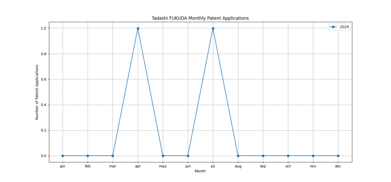
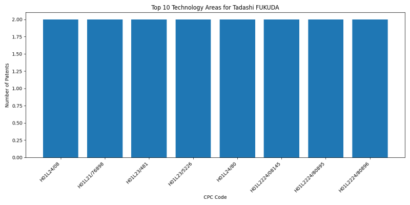
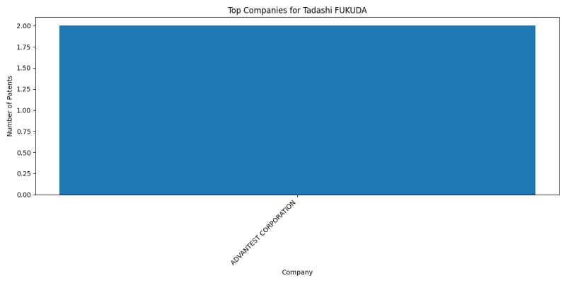
Tadashi FUKUDA is an inventor who has filed 2 patents. Their primary areas of innovation include SEMICONDUCTOR DEVICES NOT COVERED BY CLASS (2 patents), {formed through a semiconductor substrate} (2 patents), Arrangements for conducting electric current to or from the solid state body in operation, e.g. leads, terminal arrangements {; Selection of materials therefor} (2 patents), and they have worked with companies such as ADVANTEST CORPORATION (2 patents). Their most frequent collaborators include (2 collaborations), (2 collaborations), (2 collaborations).
Patent Filing Activity
Technology Areas
List of Technology Areas
- H01L24/08 (SEMICONDUCTOR DEVICES NOT COVERED BY CLASS): 2 patents
- H01L21/76898 ({formed through a semiconductor substrate}): 2 patents
- H01L23/481 (Arrangements for conducting electric current to or from the solid state body in operation, e.g. leads, terminal arrangements {; Selection of materials therefor}): 2 patents
- H01L23/5226 (SEMICONDUCTOR DEVICES NOT COVERED BY CLASS): 2 patents
- H01L24/80 ({Methods for connecting semiconductor or other solid state bodies using means for bonding being attached to, or being formed on, the surface to be connected}): 2 patents
- H01L2224/08145 (SEMICONDUCTOR DEVICES NOT COVERED BY CLASS): 2 patents
- H01L2224/80895 (SEMICONDUCTOR DEVICES NOT COVERED BY CLASS): 2 patents
- H01L2224/80896 (SEMICONDUCTOR DEVICES NOT COVERED BY CLASS): 2 patents
Companies
List of Companies
- ADVANTEST CORPORATION: 2 patents
Collaborators
- Shinji SUGATANI (2 collaborations)
- Takayuki OHBA (2 collaborations)
- Norio CHUJO (2 collaborations)
- Koji SAKUI (2 collaborations)
Subcategories
This category has the following 5 subcategories, out of 5 total.


