Category:Lin-Yu HUANG
Jump to navigation
Jump to search
Contents
Lin-Yu HUANG
Executive Summary
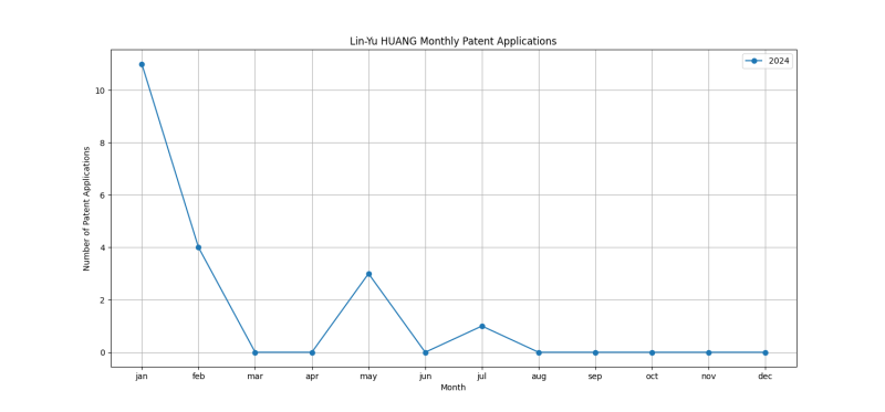
Lin-Yu HUANG is an inventor who has filed 19 patents. Their primary areas of innovation include SEMICONDUCTOR DEVICES NOT COVERED BY CLASS (8 patents), SEMICONDUCTOR DEVICES NOT COVERED BY CLASS (7 patents), SEMICONDUCTOR DEVICES NOT COVERED BY CLASS (7 patents), and they have worked with companies such as Taiwan Semiconductor Manufacturing Company, Ltd. (10 patents), TAIWAN SEMICONDUCTOR MANUFACTURING COMPANY, LTD. (9 patents). Their most frequent collaborators include (10 collaborations), (8 collaborations), (8 collaborations).
Patent Filing Activity
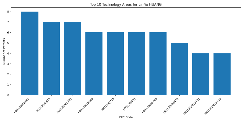
Technology Areas
List of Technology Areas
- H01L29/42392 (SEMICONDUCTOR DEVICES NOT COVERED BY CLASS): 8 patents
- H01L29/0673 (SEMICONDUCTOR DEVICES NOT COVERED BY CLASS): 7 patents
- H01L29/41791 (SEMICONDUCTOR DEVICES NOT COVERED BY CLASS): 7 patents
- H01L29/78696 (SEMICONDUCTOR DEVICES NOT COVERED BY CLASS): 6 patents
- H01L29/775 (SEMICONDUCTOR DEVICES NOT COVERED BY CLASS): 6 patents
- H01L29/401 (SEMICONDUCTOR DEVICES NOT COVERED BY CLASS): 6 patents
- H01L29/66795 (SEMICONDUCTOR DEVICES NOT COVERED BY CLASS): 6 patents
- H01L29/66439 (SEMICONDUCTOR DEVICES NOT COVERED BY CLASS): 5 patents
- H01L21/823431 (to produce devices, e.g. integrated circuits, each consisting of a plurality of components): 4 patents
- H01L21/823418 (to produce devices, e.g. integrated circuits, each consisting of a plurality of components): 4 patents
- H01L29/0649 (SEMICONDUCTOR DEVICES NOT COVERED BY CLASS): 3 patents
- H01L21/823412 (to produce devices, e.g. integrated circuits, each consisting of a plurality of components): 3 patents
- H01L29/66742 (SEMICONDUCTOR DEVICES NOT COVERED BY CLASS): 3 patents
- H01L23/481 (Arrangements for conducting electric current to or from the solid state body in operation, e.g. leads, terminal arrangements {; Selection of materials therefor}): 3 patents
- H01L29/0847 (SEMICONDUCTOR DEVICES NOT COVERED BY CLASS): 3 patents
- H01L27/0886 (SEMICONDUCTOR DEVICES NOT COVERED BY CLASS): 3 patents
- H01L21/823437 (to produce devices, e.g. integrated circuits, each consisting of a plurality of components): 2 patents
- H01L21/764 (Making of isolation regions between components): 2 patents
- H01L21/823481 (to produce devices, e.g. integrated circuits, each consisting of a plurality of components): 2 patents
- H01L29/78618 (SEMICONDUCTOR DEVICES NOT COVERED BY CLASS): 2 patents
- H01L29/41733 (SEMICONDUCTOR DEVICES NOT COVERED BY CLASS): 2 patents
- H01L23/5226 (SEMICONDUCTOR DEVICES NOT COVERED BY CLASS): 2 patents
- H01L23/5283 ({Geometry or} layout of the interconnection structure {(): 2 patents
- H01L29/45 (SEMICONDUCTOR DEVICES NOT COVERED BY CLASS): 2 patents
- H01L21/76898 ({formed through a semiconductor substrate}): 2 patents
- H01L29/7851 (SEMICONDUCTOR DEVICES NOT COVERED BY CLASS): 2 patents
- H01L29/6653 ({using self aligned silicidation, i.e. salicide (formation of conductive layers comprising silicides): 2 patents
- H01L29/66545 ({using a dummy, i.e. replacement gate in a process wherein at least a part of the final gate is self aligned to the dummy gate}): 2 patents
- H01L29/785 (SEMICONDUCTOR DEVICES NOT COVERED BY CLASS): 2 patents
- H01L21/31105 ({Etching inorganic layers}): 2 patents
- H01L21/28123 ({Lithography-related aspects, e.g. sub-lithography lengths; Isolation-related aspects, e.g. to solve problems arising at the crossing with the side of the device isolation; Planarisation aspects}): 1 patents
- H01L27/088 (SEMICONDUCTOR DEVICES NOT COVERED BY CLASS): 1 patents
- H01L21/02603 (SEMICONDUCTOR DEVICES NOT COVERED BY CLASS): 1 patents
- H01L29/66553 ({using self aligned silicidation, i.e. salicide (formation of conductive layers comprising silicides): 1 patents
- H01L29/0653 (SEMICONDUCTOR DEVICES NOT COVERED BY CLASS): 1 patents
- H01L29/7853 (SEMICONDUCTOR DEVICES NOT COVERED BY CLASS): 1 patents
- H01L23/5329 (SEMICONDUCTOR DEVICES NOT COVERED BY CLASS): 1 patents
- H01L21/823468 (to produce devices, e.g. integrated circuits, each consisting of a plurality of components): 1 patents
- H01L29/6681 (SEMICONDUCTOR DEVICES NOT COVERED BY CLASS): 1 patents
- H01L45/1683 (SEMICONDUCTOR DEVICES NOT COVERED BY CLASS): 1 patents
- H01L27/2436 (SEMICONDUCTOR DEVICES NOT COVERED BY CLASS): 1 patents
- H01L45/08 (SEMICONDUCTOR DEVICES NOT COVERED BY CLASS): 1 patents
- H01L45/1233 (SEMICONDUCTOR DEVICES NOT COVERED BY CLASS): 1 patents
- H01L45/1253 (SEMICONDUCTOR DEVICES NOT COVERED BY CLASS): 1 patents
- H01L21/02532 (SEMICONDUCTOR DEVICES NOT COVERED BY CLASS): 1 patents
- H01L21/32134 ({by liquid etching only}): 1 patents
- H01L21/32139 ({using masks}): 1 patents
- H01L29/6656 ({using self aligned silicidation, i.e. salicide (formation of conductive layers comprising silicides): 1 patents
- H01L29/66636 (SEMICONDUCTOR DEVICES NOT COVERED BY CLASS): 1 patents
- H01L29/7848 (SEMICONDUCTOR DEVICES NOT COVERED BY CLASS): 1 patents
- H01L21/02164 ({the material being a silicon oxide, e.g. SiO): 1 patents
- H01L21/31116 ({by dry-etching}): 1 patents
- H01L21/28562 (from a gas or vapour, e.g. condensation): 1 patents
- H01L21/76816 ({Aspects relating to the layout of the pattern or to the size of vias or trenches (layout of the interconnections per se): 1 patents
- H01L21/76843 ({formed in openings in a dielectric}): 1 patents
- H01L21/76852 ({the layer also covering the sidewalls of the conductive structure}): 1 patents
- H01L21/76879 ({by selective deposition of conductive material in the vias, e.g. selective C.V.D. on semiconductor material, plating (plating on semiconductors in general): 1 patents
- H01L21/823475 (to produce devices, e.g. integrated circuits, each consisting of a plurality of components): 1 patents
- H01L24/83 (SEMICONDUCTOR DEVICES NOT COVERED BY CLASS): 1 patents
- H01L24/32 (SEMICONDUCTOR DEVICES NOT COVERED BY CLASS): 1 patents
- H01L25/0657 (SEMICONDUCTOR DEVICES NOT COVERED BY CLASS): 1 patents
- H01L24/29 (SEMICONDUCTOR DEVICES NOT COVERED BY CLASS): 1 patents
- H01L21/0245 (SEMICONDUCTOR DEVICES NOT COVERED BY CLASS): 1 patents
- H01L21/26533 (producing ion implantation): 1 patents
- H01L24/16 (SEMICONDUCTOR DEVICES NOT COVERED BY CLASS): 1 patents
- H01L23/49894 (Leads, {i.e. metallisations or lead-frames} on insulating substrates, {e.g. chip carriers (shape of the substrate): 1 patents
- H01L23/49838 (Leads, {i.e. metallisations or lead-frames} on insulating substrates, {e.g. chip carriers (shape of the substrate): 1 patents
- H01L23/49816 (Leads, {i.e. metallisations or lead-frames} on insulating substrates, {e.g. chip carriers (shape of the substrate): 1 patents
- H01L23/49822 ({Multilayer substrates (multilayer metallisation on monolayer substrate): 1 patents
- H01L23/5386 (the interconnection structure between a plurality of semiconductor chips being formed on, or in, insulating substrates ({): 1 patents
- H01L23/5389 (the interconnection structure between a plurality of semiconductor chips being formed on, or in, insulating substrates ({): 1 patents
- H01L2225/06524 (SEMICONDUCTOR DEVICES NOT COVERED BY CLASS): 1 patents
- H01L2225/06541 (SEMICONDUCTOR DEVICES NOT COVERED BY CLASS): 1 patents
- H01L2225/06517 (SEMICONDUCTOR DEVICES NOT COVERED BY CLASS): 1 patents
- H01L2225/06593 (SEMICONDUCTOR DEVICES NOT COVERED BY CLASS): 1 patents
- H01L2924/37001 (SEMICONDUCTOR DEVICES NOT COVERED BY CLASS): 1 patents
- H01L2224/29187 (SEMICONDUCTOR DEVICES NOT COVERED BY CLASS): 1 patents
- H01L2224/83005 (SEMICONDUCTOR DEVICES NOT COVERED BY CLASS): 1 patents
- H01L2224/8313 (SEMICONDUCTOR DEVICES NOT COVERED BY CLASS): 1 patents
- H01L2224/83123 (SEMICONDUCTOR DEVICES NOT COVERED BY CLASS): 1 patents
- H01L2224/8383 (SEMICONDUCTOR DEVICES NOT COVERED BY CLASS): 1 patents
- H01L2224/32145 (SEMICONDUCTOR DEVICES NOT COVERED BY CLASS): 1 patents
- H01L2224/16227 (SEMICONDUCTOR DEVICES NOT COVERED BY CLASS): 1 patents
- H01L21/4857 (Manufacture or treatment of parts, e.g. containers, prior to assembly of the devices, using processes not provided for in a single one of the subgroups): 1 patents
- H01L29/0665 (SEMICONDUCTOR DEVICES NOT COVERED BY CLASS): 1 patents
- H01L21/28518 (from a gas or vapour, e.g. condensation): 1 patents
- H01L21/31111 ({by chemical means}): 1 patents
- H01L21/823821 (to produce devices, e.g. integrated circuits, each consisting of a plurality of components): 1 patents
- H01L29/4975 (SEMICONDUCTOR DEVICES NOT COVERED BY CLASS): 1 patents
- H01L2029/7858 (SEMICONDUCTOR DEVICES NOT COVERED BY CLASS): 1 patents
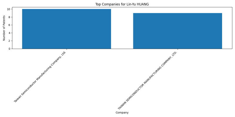
Companies
List of Companies
- Taiwan Semiconductor Manufacturing Company, Ltd.: 10 patents
- TAIWAN SEMICONDUCTOR MANUFACTURING COMPANY, LTD.: 9 patents
Collaborators
- Chih-Hao WANG (10 collaborations)
- Huan-Chieh SU (8 collaborations)
- Li-Zhen YU (8 collaborations)
- Wen-Ting LAN (4 collaborations)
- Cheng-Chi CHUANG (4 collaborations)
- Lo-Heng CHANG (3 collaborations)
- Yi-Bo LIAO (3 collaborations)
- Sheng-Tsung WANG (3 collaborations)
- Chun-Yuan CHEN (2 collaborations)
- Chung-Liang CHENG (2 collaborations)
- Meng-Huan JAO (2 collaborations)
- Chia-Hung CHU (2 collaborations)
- Shuen-Shin LIANG (2 collaborations)
- Pinyen LIN (2 collaborations)
- Shi-Ning JU (2 collaborations)
- Kuo-Cheng CHIANG (2 collaborations)
- Yu-Ming LIN (2 collaborations)
- Po-Chin CHANG (1 collaborations)
- Yuting CHENG (1 collaborations)
- Hsu-Kai CHANG (1 collaborations)
- Tzu-Pei CHEN (1 collaborations)
- Sung-Li WANG (1 collaborations)
- Yun-Ju FAN (1 collaborations)
- Huang-Lin CHAO (1 collaborations)
- Jia-Chuan YOU (1 collaborations)
- Chia-Hao CHANG (1 collaborations)
- Tien-Lu LIN (1 collaborations)
- Yi-Hsun CHIU (1 collaborations)
- I-Han HUANG (1 collaborations)
- Fu-Cheng CHANG (1 collaborations)
- Min-Hsuan LU (1 collaborations)
- Shih-Chuan CHIU (1 collaborations)
- CHIH-HAO WANG (1 collaborations)
- Yu-Xuan HUANG (1 collaborations)
Subcategories
This category has the following 2 subcategories, out of 2 total.
Categories:
- Chih-Hao WANG
- Huan-Chieh SU
- Li-Zhen YU
- Wen-Ting LAN
- Cheng-Chi CHUANG
- Lo-Heng CHANG
- Yi-Bo LIAO
- Sheng-Tsung WANG
- Chun-Yuan CHEN
- Chung-Liang CHENG
- Meng-Huan JAO
- Chia-Hung CHU
- Shuen-Shin LIANG
- Pinyen LIN
- Shi-Ning JU
- Kuo-Cheng CHIANG
- Yu-Ming LIN
- Po-Chin CHANG
- Yuting CHENG
- Hsu-Kai CHANG
- Tzu-Pei CHEN
- Sung-Li WANG
- Yun-Ju FAN
- Huang-Lin CHAO
- Jia-Chuan YOU
- Chia-Hao CHANG
- Tien-Lu LIN
- Yi-Hsun CHIU
- I-Han HUANG
- Fu-Cheng CHANG
- Min-Hsuan LU
- Shih-Chuan CHIU
- CHIH-HAO WANG
- Yu-Xuan HUANG
- Lin-Yu HUANG
- Inventors
- Inventors filing patents with Taiwan Semiconductor Manufacturing Company, Ltd.
- Inventors filing patents with TAIWAN SEMICONDUCTOR MANUFACTURING COMPANY, LTD.


