Category:John D. Hopkins of Meridian ID (US)
Revision as of 03:23, 26 July 2024 by Wikipatents (talk | contribs) (Updating Category:John_D._Hopkins_of_Meridian_ID_(US))
Contents
John D. Hopkins of Meridian ID (US)
Executive Summary
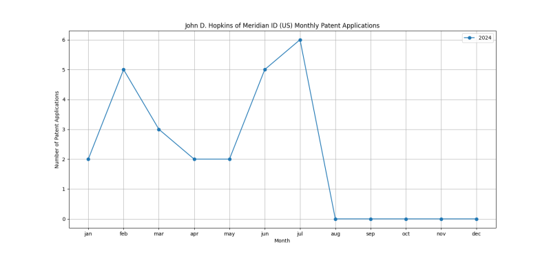
John D. Hopkins of Meridian ID (US) is an inventor who has filed 25 patents. Their primary areas of innovation include ELECTRONIC MEMORY DEVICES (14 patents), ELECTRONIC MEMORY DEVICES (14 patents), SEMICONDUCTOR DEVICES NOT COVERED BY CLASS (9 patents), and they have worked with companies such as Micron Technology, Inc. (25 patents). Their most frequent collaborators include (11 collaborations), (10 collaborations), (3 collaborations).
Patent Filing Activity
Technology Areas
List of Technology Areas
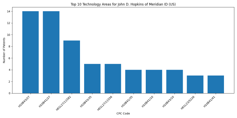
- H10B43/27 (ELECTRONIC MEMORY DEVICES): 14 patents
- H10B41/27 (ELECTRONIC MEMORY DEVICES): 14 patents
- H01L27/11582 (SEMICONDUCTOR DEVICES NOT COVERED BY CLASS): 9 patents
- H10B43/35 (ELECTRONIC MEMORY DEVICES): 5 patents
- H01L27/11556 (SEMICONDUCTOR DEVICES NOT COVERED BY CLASS): 5 patents
- H10B41/35 (ELECTRONIC MEMORY DEVICES): 4 patents
- H10B41/10 (ELECTRONIC MEMORY DEVICES): 4 patents
- H10B43/10 (ELECTRONIC MEMORY DEVICES): 4 patents
- H01L23/5226 (SEMICONDUCTOR DEVICES NOT COVERED BY CLASS): 3 patents
- H10B41/41 (ELECTRONIC MEMORY DEVICES): 3 patents
- H10B43/40 (ELECTRONIC MEMORY DEVICES): 3 patents
- G11C16/0483 ({comprising cells having several storage transistors connected in series}): 3 patents
- H01L23/535 (including internal interconnections, e.g. cross-under constructions {(internal lead connections): 3 patents
- H01L27/11565 (SEMICONDUCTOR DEVICES NOT COVERED BY CLASS): 3 patents
- H01L27/1157 (SEMICONDUCTOR DEVICES NOT COVERED BY CLASS): 3 patents
- G11C5/06 (STATIC STORES (semiconductor memory devices): 2 patents
- H01L29/40117 (SEMICONDUCTOR DEVICES NOT COVERED BY CLASS): 2 patents
- H01L21/28518 (from a gas or vapour, e.g. condensation): 2 patents
- H01L27/11524 (SEMICONDUCTOR DEVICES NOT COVERED BY CLASS): 2 patents
- H10B41/50 (ELECTRONIC MEMORY DEVICES): 2 patents
- H10B43/50 (ELECTRONIC MEMORY DEVICES): 2 patents
- H01L27/11519 (SEMICONDUCTOR DEVICES NOT COVERED BY CLASS): 2 patents
- H01L21/2254 ({from or through or into an applied layer, e.g. photoresist, nitrides}): 1 patents
- H01L23/562 (SEMICONDUCTOR DEVICES NOT COVERED BY CLASS): 1 patents
- H01L21/31053 ({involving a dielectric removal step}): 1 patents
- H01L21/31144 ({using masks}): 1 patents
- H01L21/76224 ({using trench refilling with dielectric materials (trench filling with polycristalline silicon): 1 patents
- H01L29/40114 (SEMICONDUCTOR DEVICES NOT COVERED BY CLASS): 1 patents
- H01L29/42328 (SEMICONDUCTOR DEVICES NOT COVERED BY CLASS): 1 patents
- H01L29/42344 (SEMICONDUCTOR DEVICES NOT COVERED BY CLASS): 1 patents
- H01L21/76895 (Applying interconnections to be used for carrying current between separate components within a device {comprising conductors and dielectrics}): 1 patents
- H01L21/76805 ({the opening being a via or contact hole penetrating the underlying conductor}): 1 patents
- H01L21/76829 ({characterised by the formation of thin functional dielectric layers, e.g. dielectric etch-stop, barrier, capping or liner layers}): 1 patents
- H01L21/76802 (Applying interconnections to be used for carrying current between separate components within a device {comprising conductors and dielectrics}): 1 patents
- H01L21/76889 ({by deposition over sacrificial masking layer, e.g. lift-off (lift-off per se): 1 patents
- H01L27/11553 (SEMICONDUCTOR DEVICES NOT COVERED BY CLASS): 1 patents
- G11C5/025 ({Geometric lay-out considerations of storage- and peripheral-blocks in a semiconductor storage device (geometrical lay-out of the components in integrated circuits,): 1 patents
- H01L21/768 (Applying interconnections to be used for carrying current between separate components within a device {comprising conductors and dielectrics}): 1 patents
- H01L21/31111 ({by chemical means}): 1 patents
- H01L21/31155 (Doping the insulating layers): 1 patents
- H01L21/32134 ({by liquid etching only}): 1 patents
- H01L21/32155 (Doping the layers): 1 patents
- H01L23/5283 ({Geometry or} layout of the interconnection structure {(): 1 patents
- H01L21/30608 ({Anisotropic liquid etching (): 1 patents
- H01L21/3086 ({characterised by the process involved to create the mask, e.g. lift-off masks, sidewalls, or to modify the mask, e.g. pre-treatment, post-treatment}): 1 patents
- H01L27/11578 (SEMICONDUCTOR DEVICES NOT COVERED BY CLASS): 1 patents
- H01L27/11543 (SEMICONDUCTOR DEVICES NOT COVERED BY CLASS): 1 patents
Companies
List of Companies
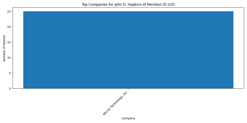
- Micron Technology, Inc.: 25 patents
Collaborators
- Alyssa N. Scarbrough of Boise ID (US) (11 collaborations)
- Jordan D. Greenlee of Boise ID (US) (10 collaborations)
- Darwin A. Clampitt of Wilder ID (US) (3 collaborations)
- Nancy M. Lomeli of Boise ID (US) (3 collaborations)
- Shuangqiang Luo of Boise ID (US) (2 collaborations)
- Matthew J. King of Boise ID (US) (1 collaborations)
- Roger W. Lindsay of Boise ID (US) (1 collaborations)
- Kevin Y. Titus of Meridian ID (US) (1 collaborations)
- Rohit Kothari of Boise ID (US) (1 collaborations)
- Adam L. Olson of Boise ID (US) (1 collaborations)
- Jeslin J. Wu of Boise ID (US) (1 collaborations)
- Sidhartha Gupta of Boise ID (US) (1 collaborations)
- Adam W. Saxler of Boise ID (US) (1 collaborations)
- Andrew Li of Boise ID (US) (1 collaborations)
- Andrew L. Li of Boise ID (US) (1 collaborations)
- Michael J. Puett of Boise ID (US) (1 collaborations)
- Christopher R. Ritchie of Boise ID (US) (1 collaborations)
- Lifang Xu of Boise ID (US) (1 collaborations)
- Indra V. Chary of Boise ID (US) (1 collaborations)
- Kar Wui Thong of Boise ID (US) (1 collaborations)
- Shicong Wang of Meridain ID (US) (1 collaborations)
Subcategories
This category has the following 3 subcategories, out of 3 total.
J
L
S
Pages in category "John D. Hopkins of Meridian ID (US)"
The following 34 pages are in this category, out of 34 total.
1
- 17823276. ELECTRONIC DEVICES COMPRISING BLOCKING REGIONS, AND RELATED ELECTRONIC SYSTEMS AND METHODS simplified abstract (Micron Technology, Inc.)
- 17830108. Memory Arrays Comprising Strings Of Memory Cells And Methods Used In Forming A Memory Array Comprising Strings Of Memory Cells simplified abstract (Micron Technology, Inc.)
- 17851865. Memory Arrays Comprising Strings Of Memory Cells And Methods Used In Forming A Memory Array Comprising Strings Of Memory Cells simplified abstract (Micron Technology, Inc.)
- 17897350. Memory Circuitry And Method Used In Forming Memory Circuitry simplified abstract (Micron Technology, Inc.)
- 17897399. Memory Circuitry And Method Used In Forming Memory Circuitry simplified abstract (Micron Technology, Inc.)
- 17897460. Memory Circuitry And Method Used In Forming Memory Circuitry simplified abstract (Micron Technology, Inc.)
- 17897516. Memory Circuitry And Method Used In Forming Memory Circuitry simplified abstract (Micron Technology, Inc.)
- 18244169. Integrated Circuitry Comprising A Memory Array Comprising Strings Of Memory Cells And Methods Used In Forming A Memory Array Comprising Strings Of Memory Cells simplified abstract (MICRON TECHNOLOGY, INC.)
- 18324084. MICROELECTRONIC DEVICES COMPRISING A BORON-CONTAINING MATERIAL, AND RELATED ELECTRONIC SYSTEMS AND METHODS simplified abstract (Micron Technology, Inc.)
- 18397059. Memory Arrays Comprising Strings Of Memory Cells And Methods Used In Forming A Memory Array Comprising Strings Of Memory Cells simplified abstract (Micron Technology, Inc.)
- 18415928. Integrated Assemblies and Methods of Forming Integrated Assemblies simplified abstract (Micron Technology, Inc.)
- 18428836. METHODS OF FORMING MICROELECTRONIC DEVICES simplified abstract (Micron Technology, Inc.)
- 18581667. MICROELECTRONIC DEVICES WITH SOURCE REGION VERTICALLY BETWEEN TIERED DECKS, AND RELATED METHODS simplified abstract (Micron Technology, Inc.)
- 18584275. Integrated Assemblies and Methods of Forming Integrated Assemblies simplified abstract (Micron Technology, Inc.)
- 18585372. Integrated Assemblies and Methods of Forming Integrated Assemblies simplified abstract (Micron Technology, Inc.)
- 18597695. Integrated Circuitry Comprising A Memory Array Comprising Strings Of Memory Cells And Method Used In Forming A Memory Array Comprising Strings Of Memory Cells simplified abstract (Micron Technology, Inc.)
- 18604811. Integrated Assemblies, and Methods of Forming Integrated Assemblies simplified abstract (MICRON TECHNOLOGY, INC.)
- 18620002. Memory Array And Method Used In Forming A Memory Array Comprising Strings Of Memory Cells simplified abstract (Micron Technology, Inc.)
- 18745872. METHODS OF FORMING MICROELECTRONIC DEVICES INCLUDING VOIDS NEIGHBORING CONDUCTIVE CONTACTS, AND RELATED ELECTRONIC SYSTEMS simplified abstract (Micron Technology, Inc.)
M
- Micron technology, inc. (20240130121). MICROELECTRONIC DEVICES INCLUDING A DOPED DIELECTRIC MATERIAL, METHODS OF FORMING THE MICROELECTRONIC DEVICES, AND RELATED SYSTEMS simplified abstract
- Micron technology, inc. (20240164093). Integrated Assemblies and Methods of Forming Integrated Assemblies simplified abstract
- Micron technology, inc. (20240186267). SEMICONDUCTOR DEVICES COMPRISING STEPS simplified abstract
- Micron technology, inc. (20240203496). Memory Array Comprising Strings Of Memory Cells And Methods Including A Method Used In Forming A Memory Array Comprising Strings Of Memory Cells simplified abstract
- Micron technology, inc. (20240203791). Integrated Circuitry, A Memory Array Comprising Strings Of Memory Cells, A Method Used In Forming A Conductive Via, A Method Used In Forming A Memory Array Comprising Strings Of Memory Cells simplified abstract
- Micron technology, inc. (20240206175). Memory Circuitry And Method Used In Forming Memory Circuitry simplified abstract
- Micron technology, inc. (20240224524). Integrated Assemblies, and Methods of Forming Integrated Assemblies simplified abstract
- Micron technology, inc. (20240237352). MICROELECTRONIC DEVICES WITH SOURCE REGION VERTICALLY BETWEEN TIERED DECKS, AND RELATED METHODS simplified abstract
- Micron technology, inc. (20240244840). Memory Array And Method Used In Forming A Memory Array Comprising Strings Of Memory Cells simplified abstract
- Micron technology, inc. (20240251554). Integrated Assemblies and Methods of Forming Integrated Assemblies simplified abstract
- Micron technology, inc. (20240251555). Integrated Assemblies and Methods of Forming Integrated Assemblies simplified abstract
- Micron technology, inc. (20240251556). Integrated Circuitry Comprising A Memory Array Comprising Strings Of Memory Cells And Method Used In Forming A Memory Array Comprising Strings Of Memory Cells simplified abstract
- Micron technology, inc. (20240339357). METHODS OF FORMING MICROELECTRONIC DEVICES INCLUDING VOIDS NEIGHBORING CONDUCTIVE CONTACTS, AND RELATED ELECTRONIC SYSTEMS simplified abstract
Categories:
- Alyssa N. Scarbrough of Boise ID (US)
- Jordan D. Greenlee of Boise ID (US)
- Darwin A. Clampitt of Wilder ID (US)
- Nancy M. Lomeli of Boise ID (US)
- Shuangqiang Luo of Boise ID (US)
- Matthew J. King of Boise ID (US)
- Roger W. Lindsay of Boise ID (US)
- Kevin Y. Titus of Meridian ID (US)
- Rohit Kothari of Boise ID (US)
- Adam L. Olson of Boise ID (US)
- Jeslin J. Wu of Boise ID (US)
- Sidhartha Gupta of Boise ID (US)
- Adam W. Saxler of Boise ID (US)
- Andrew Li of Boise ID (US)
- Andrew L. Li of Boise ID (US)
- Michael J. Puett of Boise ID (US)
- Christopher R. Ritchie of Boise ID (US)
- Lifang Xu of Boise ID (US)
- Indra V. Chary of Boise ID (US)
- Kar Wui Thong of Boise ID (US)
- Shicong Wang of Meridain ID (US)
- John D. Hopkins of Meridian ID (US)
- Inventors
- Inventors filing patents with Micron Technology, Inc.


