Category:Takayuki NEGISHI
Revision as of 08:52, 19 July 2024 by Wikipatents (talk | contribs) (Updating Category:Takayuki_NEGISHI)
Contents
Takayuki NEGISHI
Executive Summary
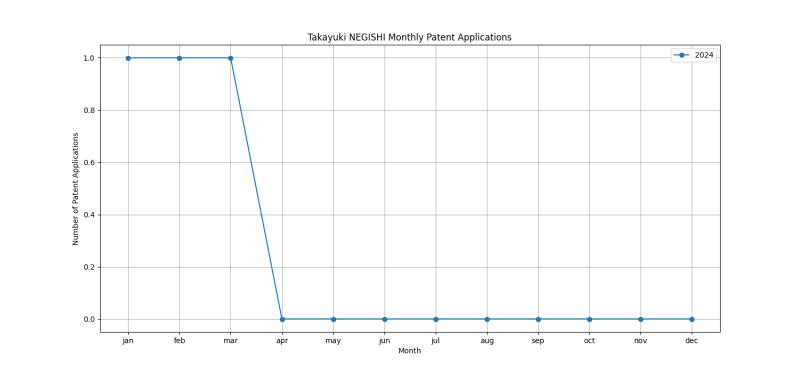
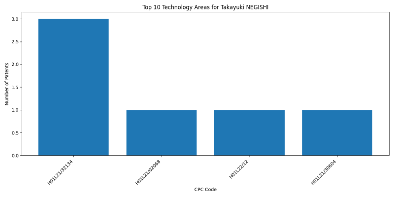
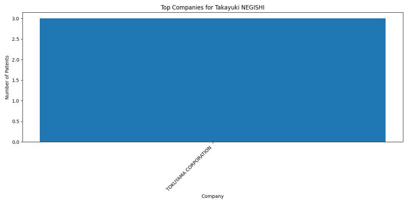
Takayuki NEGISHI is an inventor who has filed 3 patents. Their primary areas of innovation include {by liquid etching only} (3 patents), {during, before or after processing of insulating layers} (1 patents), {for structural parameters, e.g. thickness, line width, refractive index, temperature, warp, bond strength, defects, optical inspection, electrical measurement of structural dimensions, metallurgic measurement of diffusions (electrical measurement of diffusions (1 patents), and they have worked with companies such as TOKUYAMA CORPORATION (3 patents). Their most frequent collaborators include (3 collaborations), (3 collaborations), (2 collaborations).
Patent Filing Activity
Technology Areas
List of Technology Areas
- H01L21/32134 ({by liquid etching only}): 3 patents
- H01L21/02068 ({during, before or after processing of insulating layers}): 1 patents
- H01L22/12 ({for structural parameters, e.g. thickness, line width, refractive index, temperature, warp, bond strength, defects, optical inspection, electrical measurement of structural dimensions, metallurgic measurement of diffusions (electrical measurement of diffusions): 1 patents
- H01L21/30604 (Chemical or electrical treatment, e.g. electrolytic etching (to form insulating layers): 1 patents
Companies
List of Companies
- TOKUYAMA CORPORATION: 3 patents
Collaborators
- Yuki KIKKAWA (3 collaborations)
- Tomoaki SATO (3 collaborations)
- Takafumi SHIMODA (2 collaborations)
- Kohei SAITO (2 collaborations)
- Hiroto YARIMIZU (1 collaborations)
Subcategories
This category has the following 5 subcategories, out of 5 total.


