Category:Jeremy Alfred Theil of Mountain View CA (US)
Appearance
Jeremy Alfred Theil of Mountain View CA (US)
Executive Summary
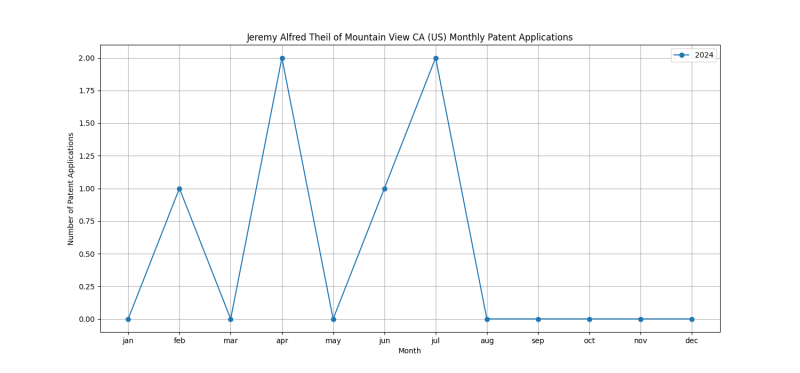
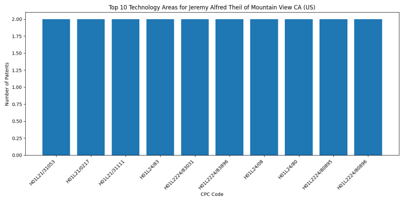
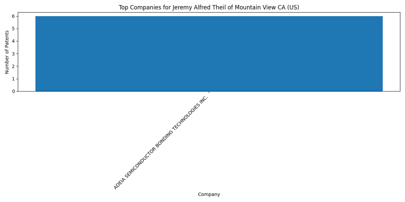
Jeremy Alfred Theil of Mountain View CA (US) is an inventor who has filed 6 patents. Their primary areas of innovation include {involving a dielectric removal step} (2 patents), {the material being a silicon nitride not containing oxygen, e.g. SixNy or SixByNz ( (2 patents), {by chemical means} (2 patents), and they have worked with companies such as ADEIA SEMICONDUCTOR BONDING TECHNOLOGIES INC. (6 patents). Their most frequent collaborators include (4 collaborations), (2 collaborations), (2 collaborations).
Patent Filing Activity
Technology Areas
List of Technology Areas
- H01L21/31053 ({involving a dielectric removal step}): 2 patents
- H01L21/0217 ({the material being a silicon nitride not containing oxygen, e.g. SixNy or SixByNz (): 2 patents
- H01L21/31111 ({by chemical means}): 2 patents
- H01L24/83 (SEMICONDUCTOR DEVICES NOT COVERED BY CLASS): 2 patents
- H01L2224/83031 (SEMICONDUCTOR DEVICES NOT COVERED BY CLASS): 2 patents
- H01L2224/83896 (SEMICONDUCTOR DEVICES NOT COVERED BY CLASS): 2 patents
- H01L24/08 (SEMICONDUCTOR DEVICES NOT COVERED BY CLASS): 2 patents
- H01L24/80 ({Methods for connecting semiconductor or other solid state bodies using means for bonding being attached to, or being formed on, the surface to be connected}): 2 patents
- H01L2224/80895 (SEMICONDUCTOR DEVICES NOT COVERED BY CLASS): 2 patents
- H01L2224/80896 (SEMICONDUCTOR DEVICES NOT COVERED BY CLASS): 2 patents
- H01L24/05 (SEMICONDUCTOR DEVICES NOT COVERED BY CLASS): 1 patents
- H01L24/03 (SEMICONDUCTOR DEVICES NOT COVERED BY CLASS): 1 patents
- H01L2224/03462 (SEMICONDUCTOR DEVICES NOT COVERED BY CLASS): 1 patents
- H01L2224/03616 (SEMICONDUCTOR DEVICES NOT COVERED BY CLASS): 1 patents
- H01L2224/05147 (SEMICONDUCTOR DEVICES NOT COVERED BY CLASS): 1 patents
- H01L2224/08145 (SEMICONDUCTOR DEVICES NOT COVERED BY CLASS): 1 patents
- H01L2924/3512 (SEMICONDUCTOR DEVICES NOT COVERED BY CLASS): 1 patents
- H01L25/0657 (SEMICONDUCTOR DEVICES NOT COVERED BY CLASS): 1 patents
- H01L21/76898 ({formed through a semiconductor substrate}): 1 patents
- H01L23/5384 ({Conductive vias through the substrate with or without pins, e.g. buried coaxial conductors (): 1 patents
- H01L23/5385 (the interconnection structure between a plurality of semiconductor chips being formed on, or in, insulating substrates ({): 1 patents
- H01L23/5386 (the interconnection structure between a plurality of semiconductor chips being formed on, or in, insulating substrates ({): 1 patents
- H01L24/95 (SEMICONDUCTOR DEVICES NOT COVERED BY CLASS): 1 patents
- H01L2224/08057 (SEMICONDUCTOR DEVICES NOT COVERED BY CLASS): 1 patents
- H01L2224/08147 (SEMICONDUCTOR DEVICES NOT COVERED BY CLASS): 1 patents
- H01L23/5226 (SEMICONDUCTOR DEVICES NOT COVERED BY CLASS): 1 patents
- H01L24/20 (SEMICONDUCTOR DEVICES NOT COVERED BY CLASS): 1 patents
- H01L23/298 (SEMICONDUCTOR DEVICES NOT COVERED BY CLASS): 1 patents
- H01L23/3178 ({Coating or filling in grooves made in the semiconductor body}): 1 patents
Companies
List of Companies
- ADEIA SEMICONDUCTOR BONDING TECHNOLOGIES INC.: 6 patents
Collaborators
- Cyprian Emeka Uzoh of San Jose CA (US) (4 collaborations)
- Guilian Gao of Campbell CA (US) (2 collaborations)
- Rajesh Katkar of Milpitas CA (US) (2 collaborations)
- Belgacem Haba of Saratoga CA (US) (1 collaborations)
- Guilian Gao of San Jose CA (US) (1 collaborations)
- Laura Wills Mirkarimi of Sunol CA (US) (1 collaborations)
- Gaius Gillman Fountain, Jr. of Youngsville NC (US) (1 collaborations)
Subcategories
This category has the following 7 subcategories, out of 7 total.
B
C
G
J
L
R
Categories:
- Cyprian Emeka Uzoh of San Jose CA (US)
- Guilian Gao of Campbell CA (US)
- Rajesh Katkar of Milpitas CA (US)
- Belgacem Haba of Saratoga CA (US)
- Guilian Gao of San Jose CA (US)
- Laura Wills Mirkarimi of Sunol CA (US)
- Gaius Gillman Fountain, Jr. of Youngsville NC (US)
- Jeremy Alfred Theil of Mountain View CA (US)
- Inventors
- Inventors filing patents with ADEIA SEMICONDUCTOR BONDING TECHNOLOGIES INC.


