Category:Feng-Cheng Yang
Appearance
Feng-Cheng Yang
Executive Summary
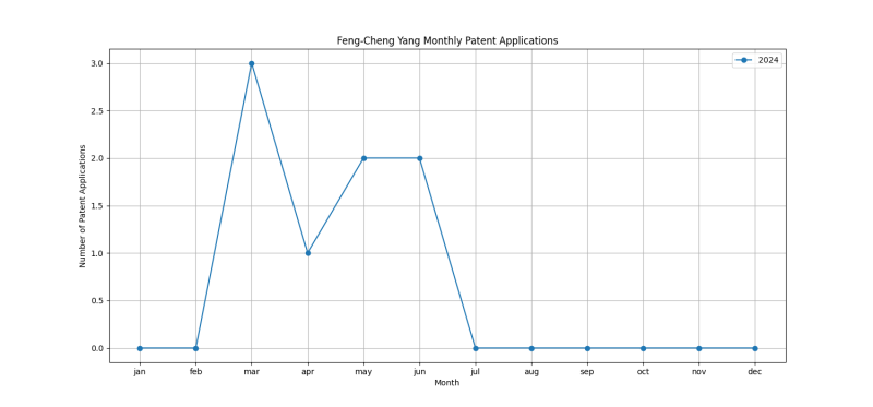
Feng-Cheng Yang is an inventor who has filed 8 patents. Their primary areas of innovation include SEMICONDUCTOR DEVICES NOT COVERED BY CLASS (3 patents), SEMICONDUCTOR DEVICES NOT COVERED BY CLASS (3 patents), SEMICONDUCTOR DEVICES NOT COVERED BY CLASS (2 patents), and they have worked with companies such as Taiwan Semiconductor Manufacturing Co., Ltd. (8 patents). Their most frequent collaborators include (5 collaborations), (4 collaborations), (3 collaborations).
Patent Filing Activity
Technology Areas
List of Technology Areas
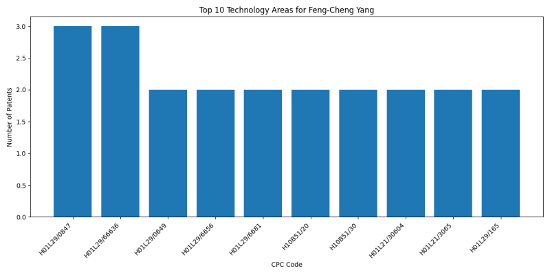
- H01L29/0847 (SEMICONDUCTOR DEVICES NOT COVERED BY CLASS): 3 patents
- H01L29/66636 (SEMICONDUCTOR DEVICES NOT COVERED BY CLASS): 3 patents
- H01L29/0649 (SEMICONDUCTOR DEVICES NOT COVERED BY CLASS): 2 patents
- H01L29/6656 ({using self aligned silicidation, i.e. salicide (formation of conductive layers comprising silicides): 2 patents
- H01L29/6681 (SEMICONDUCTOR DEVICES NOT COVERED BY CLASS): 2 patents
- H10B51/20 (ELECTRONIC MEMORY DEVICES): 2 patents
- H10B51/30 (ELECTRONIC MEMORY DEVICES): 2 patents
- H01L21/30604 (Chemical or electrical treatment, e.g. electrolytic etching (to form insulating layers): 2 patents
- H01L21/3065 (Plasma etching; Reactive-ion etching): 2 patents
- H01L29/165 (SEMICONDUCTOR DEVICES NOT COVERED BY CLASS): 2 patents
- H01L21/823821 (to produce devices, e.g. integrated circuits, each consisting of a plurality of components): 2 patents
- H01L27/0924 (SEMICONDUCTOR DEVICES NOT COVERED BY CLASS): 2 patents
- H01L21/764 (Making of isolation regions between components): 1 patents
- H01L21/7682 (Applying interconnections to be used for carrying current between separate components within a device {comprising conductors and dielectrics}): 1 patents
- H01L21/76841 (Applying interconnections to be used for carrying current between separate components within a device {comprising conductors and dielectrics}): 1 patents
- H01L21/76897 ({Formation of self-aligned vias or contact plugs, i.e. involving a lithographically uncritical step (self-aligned silicidation on field effect transistors): 1 patents
- H01L21/823864 (to produce devices, e.g. integrated circuits, each consisting of a plurality of components): 1 patents
- H01L21/823871 (to produce devices, e.g. integrated circuits, each consisting of a plurality of components): 1 patents
- H01L23/10 (SEMICONDUCTOR DEVICES NOT COVERED BY CLASS): 1 patents
- H01L29/66545 ({using a dummy, i.e. replacement gate in a process wherein at least a part of the final gate is self aligned to the dummy gate}): 1 patents
- H01L23/535 (including internal interconnections, e.g. cross-under constructions {(internal lead connections): 1 patents
- H01L29/41741 (SEMICONDUCTOR DEVICES NOT COVERED BY CLASS): 1 patents
- H01L29/41775 (SEMICONDUCTOR DEVICES NOT COVERED BY CLASS): 1 patents
- H10B51/00 (Ferroelectric RAM [FeRAM] devices comprising ferroelectric memory transistors): 1 patents
- H10B51/10 (ELECTRONIC MEMORY DEVICES): 1 patents
- H01L21/32133 ({by chemical means only}): 1 patents
- H01L21/76802 (Applying interconnections to be used for carrying current between separate components within a device {comprising conductors and dielectrics}): 1 patents
- H01L21/7684 (Applying interconnections to be used for carrying current between separate components within a device {comprising conductors and dielectrics}): 1 patents
- H01L21/76871 ({Layers specifically deposited to enhance or enable the nucleation of further layers, i.e. seed layers}): 1 patents
- H01L21/76877 ({Thin films associated with contacts of capacitors}): 1 patents
- H01L23/5226 (SEMICONDUCTOR DEVICES NOT COVERED BY CLASS): 1 patents
- H01L29/0653 (SEMICONDUCTOR DEVICES NOT COVERED BY CLASS): 1 patents
- H01L21/02057 ({Cleaning during device manufacture}): 1 patents
- H01L21/02227 ({formation by a process other than a deposition process}): 1 patents
- H01L29/66795 (SEMICONDUCTOR DEVICES NOT COVERED BY CLASS): 1 patents
- H01L29/7848 (SEMICONDUCTOR DEVICES NOT COVERED BY CLASS): 1 patents
- H01L29/7851 (SEMICONDUCTOR DEVICES NOT COVERED BY CLASS): 1 patents
- H01L21/76224 ({using trench refilling with dielectric materials (trench filling with polycristalline silicon): 1 patents
- H01L27/0886 (SEMICONDUCTOR DEVICES NOT COVERED BY CLASS): 1 patents
- H01L29/785 (SEMICONDUCTOR DEVICES NOT COVERED BY CLASS): 1 patents
- H01L2029/7858 (SEMICONDUCTOR DEVICES NOT COVERED BY CLASS): 1 patents
- H01L29/66803 (SEMICONDUCTOR DEVICES NOT COVERED BY CLASS): 1 patents
- H01L21/225 (using diffusion into or out of a solid from or into a solid phase, e.g. a doped oxide layer {(): 1 patents
- H01L21/26526 (producing ion implantation): 1 patents
- H01L29/66818 (SEMICONDUCTOR DEVICES NOT COVERED BY CLASS): 1 patents
- H10B10/12 (ELECTRONIC MEMORY DEVICES): 1 patents
- H01L21/0273 ({characterised by the treatment of photoresist layers}): 1 patents
- H01L21/31111 ({by chemical means}): 1 patents
- H01L21/31144 ({using masks}): 1 patents
- H01L21/823418 (to produce devices, e.g. integrated circuits, each consisting of a plurality of components): 1 patents
- H01L21/823431 (to produce devices, e.g. integrated circuits, each consisting of a plurality of components): 1 patents
- H01L21/823437 (to produce devices, e.g. integrated circuits, each consisting of a plurality of components): 1 patents
- H10B10/18 (ELECTRONIC MEMORY DEVICES): 1 patents
- H01L21/823814 (to produce devices, e.g. integrated circuits, each consisting of a plurality of components): 1 patents
- H01L21/308 (using masks (): 1 patents
- H01L21/823878 (to produce devices, e.g. integrated circuits, each consisting of a plurality of components): 1 patents
Companies
Error creating thumbnail: File missing
List of Companies
- Taiwan Semiconductor Manufacturing Co., Ltd.: 8 patents
Collaborators
- Yen-Ming Chen (5 collaborations)
- Sheng-Chen Wang (4 collaborations)
- Sai-Hooi Yeong (3 collaborations)
- Kai-Hsuan Lee (2 collaborations)
- Bo-Yu Lai (2 collaborations)
- Meng-Han Lin (2 collaborations)
- Han-Jong Chia (2 collaborations)
- Chung-Te Lin (2 collaborations)
- Feng-Ching Chu (2 collaborations)
- Wei-Yang Lee (2 collaborations)
- Chia-Ta Yu (2 collaborations)
- Yih-Ann Lin (1 collaborations)
- Yu-Ming Lin (1 collaborations)
- Hsiao-Chiu Hsu (1 collaborations)
- Ziwei Fang (1 collaborations)
- Cheng-Yu Yang (1 collaborations)
Subcategories
This category has the following 4 subcategories, out of 4 total.

