Category:Chih-Hao WANG
Revision as of 01:52, 19 July 2024 by Wikipatents (talk | contribs) (Updating Category:Chih-Hao_WANG)
Contents
Chih-Hao WANG
Executive Summary
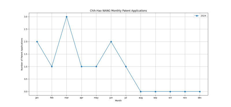
Chih-Hao WANG is an inventor who has filed 34 patents. Their primary areas of innovation include SEMICONDUCTOR DEVICES NOT COVERED BY CLASS (21 patents), SEMICONDUCTOR DEVICES NOT COVERED BY CLASS (19 patents), {using a dummy, i.e. replacement gate in a process wherein at least a part of the final gate is self aligned to the dummy gate} (17 patents), and they have worked with companies such as Taiwan Semiconductor Manufacturing Company, Ltd. (18 patents), TAIWAN SEMICONDUCTOR MANUFACTURING COMPANY, LTD. (16 patents). Their most frequent collaborators include (19 collaborations), (10 collaborations), (9 collaborations).
Patent Filing Activity
Technology Areas
List of Technology Areas
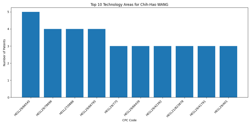
- H01L29/42392 (SEMICONDUCTOR DEVICES NOT COVERED BY CLASS): 21 patents
- H01L29/0673 (SEMICONDUCTOR DEVICES NOT COVERED BY CLASS): 19 patents
- H01L29/66545 ({using a dummy, i.e. replacement gate in a process wherein at least a part of the final gate is self aligned to the dummy gate}): 17 patents
- H01L29/78696 (SEMICONDUCTOR DEVICES NOT COVERED BY CLASS): 16 patents
- H01L21/823431 (to produce devices, e.g. integrated circuits, each consisting of a plurality of components): 12 patents
- H01L29/775 (SEMICONDUCTOR DEVICES NOT COVERED BY CLASS): 12 patents
- H01L29/66439 (SEMICONDUCTOR DEVICES NOT COVERED BY CLASS): 11 patents
- H01L29/0847 (SEMICONDUCTOR DEVICES NOT COVERED BY CLASS): 9 patents
- H01L21/823418 (to produce devices, e.g. integrated circuits, each consisting of a plurality of components): 8 patents
- H01L21/823412 (to produce devices, e.g. integrated circuits, each consisting of a plurality of components): 7 patents
- H01L21/823481 (to produce devices, e.g. integrated circuits, each consisting of a plurality of components): 7 patents
- H01L27/0886 (SEMICONDUCTOR DEVICES NOT COVERED BY CLASS): 7 patents
- H01L29/66795 (SEMICONDUCTOR DEVICES NOT COVERED BY CLASS): 7 patents
- H01L29/41791 (SEMICONDUCTOR DEVICES NOT COVERED BY CLASS): 6 patents
- H01L29/401 (SEMICONDUCTOR DEVICES NOT COVERED BY CLASS): 5 patents
- H01L29/0649 (SEMICONDUCTOR DEVICES NOT COVERED BY CLASS): 5 patents
- H01L29/66742 (SEMICONDUCTOR DEVICES NOT COVERED BY CLASS): 5 patents
- H01L29/66553 ({using self aligned silicidation, i.e. salicide (formation of conductive layers comprising silicides): 4 patents
- H01L21/823475 (to produce devices, e.g. integrated circuits, each consisting of a plurality of components): 4 patents
- H01L29/785 (SEMICONDUCTOR DEVICES NOT COVERED BY CLASS): 4 patents
- H01L29/6653 ({using self aligned silicidation, i.e. salicide (formation of conductive layers comprising silicides): 4 patents
- H01L21/823807 (to produce devices, e.g. integrated circuits, each consisting of a plurality of components): 3 patents
- H01L21/823814 (to produce devices, e.g. integrated circuits, each consisting of a plurality of components): 3 patents
- H01L27/092 (SEMICONDUCTOR DEVICES NOT COVERED BY CLASS): 3 patents
- H01L27/088 (SEMICONDUCTOR DEVICES NOT COVERED BY CLASS): 3 patents
- H01L21/02603 (SEMICONDUCTOR DEVICES NOT COVERED BY CLASS): 3 patents
- H01L21/823437 (to produce devices, e.g. integrated circuits, each consisting of a plurality of components): 3 patents
- H01L23/5226 (SEMICONDUCTOR DEVICES NOT COVERED BY CLASS): 3 patents
- H01L29/6656 ({using self aligned silicidation, i.e. salicide (formation of conductive layers comprising silicides): 3 patents
- H01L21/76224 ({using trench refilling with dielectric materials (trench filling with polycristalline silicon): 3 patents
- H01L21/28088 (Manufacture of electrodes on semiconductor bodies using processes or apparatus not provided for in groups): 2 patents
- H01L21/823878 (to produce devices, e.g. integrated circuits, each consisting of a plurality of components): 2 patents
- H01L21/823828 (to produce devices, e.g. integrated circuits, each consisting of a plurality of components): 2 patents
- H01L21/764 (Making of isolation regions between components): 2 patents
- H01L23/5283 ({Geometry or} layout of the interconnection structure {(): 2 patents
- H01L29/78618 (SEMICONDUCTOR DEVICES NOT COVERED BY CLASS): 2 patents
- H01L29/7853 (SEMICONDUCTOR DEVICES NOT COVERED BY CLASS): 2 patents
- H01L29/7848 (SEMICONDUCTOR DEVICES NOT COVERED BY CLASS): 2 patents
- H01L29/7851 (SEMICONDUCTOR DEVICES NOT COVERED BY CLASS): 2 patents
- H01L21/823468 (to produce devices, e.g. integrated circuits, each consisting of a plurality of components): 2 patents
- H01L21/32139 ({using masks}): 2 patents
- H01L21/76843 ({formed in openings in a dielectric}): 2 patents
- H01L21/31105 ({Etching inorganic layers}): 2 patents
- H01L21/823842 (to produce devices, e.g. integrated circuits, each consisting of a plurality of components): 1 patents
- H01L29/4908 (SEMICONDUCTOR DEVICES NOT COVERED BY CLASS): 1 patents
- H01L29/41733 (SEMICONDUCTOR DEVICES NOT COVERED BY CLASS): 1 patents
- H01L21/823857 (to produce devices, e.g. integrated circuits, each consisting of a plurality of components): 1 patents
- H01L21/28123 ({Lithography-related aspects, e.g. sub-lithography lengths; Isolation-related aspects, e.g. to solve problems arising at the crossing with the side of the device isolation; Planarisation aspects}): 1 patents
- H01L21/76829 ({characterised by the formation of thin functional dielectric layers, e.g. dielectric etch-stop, barrier, capping or liner layers}): 1 patents
- H01L21/76897 ({Formation of self-aligned vias or contact plugs, i.e. involving a lithographically uncritical step (self-aligned silicidation on field effect transistors): 1 patents
- H01L21/823456 (to produce devices, e.g. integrated circuits, each consisting of a plurality of components): 1 patents
- H01L29/0653 (SEMICONDUCTOR DEVICES NOT COVERED BY CLASS): 1 patents
- H01L27/0922 (SEMICONDUCTOR DEVICES NOT COVERED BY CLASS): 1 patents
- H01L29/6681 (SEMICONDUCTOR DEVICES NOT COVERED BY CLASS): 1 patents
- H01L29/45 (SEMICONDUCTOR DEVICES NOT COVERED BY CLASS): 1 patents
- H01L21/02532 (SEMICONDUCTOR DEVICES NOT COVERED BY CLASS): 1 patents
- H01L21/32134 ({by liquid etching only}): 1 patents
- H01L29/66636 (SEMICONDUCTOR DEVICES NOT COVERED BY CLASS): 1 patents
- H01L21/02164 ({the material being a silicon oxide, e.g. SiO): 1 patents
- H01L21/31116 ({by dry-etching}): 1 patents
- H01L21/28562 (from a gas or vapour, e.g. condensation): 1 patents
- H01L21/76816 ({Aspects relating to the layout of the pattern or to the size of vias or trenches (layout of the interconnections per se): 1 patents
- H01L21/76852 ({the layer also covering the sidewalls of the conductive structure}): 1 patents
- H01L21/76879 ({by selective deposition of conductive material in the vias, e.g. selective C.V.D. on semiconductor material, plating (plating on semiconductors in general): 1 patents
- H01L29/0665 (SEMICONDUCTOR DEVICES NOT COVERED BY CLASS): 1 patents
- H01L21/28575 (from a gas or vapour, e.g. condensation): 1 patents
- H01L21/30604 (Chemical or electrical treatment, e.g. electrolytic etching (to form insulating layers): 1 patents
- H01L27/0928 (SEMICONDUCTOR DEVICES NOT COVERED BY CLASS): 1 patents
- H01L21/823892 (to produce devices, e.g. integrated circuits, each consisting of a plurality of components): 1 patents
- H01L23/481 (Arrangements for conducting electric current to or from the solid state body in operation, e.g. leads, terminal arrangements {; Selection of materials therefor}): 1 patents
- H01L21/76898 ({formed through a semiconductor substrate}): 1 patents
- H01L27/1108 (SEMICONDUCTOR DEVICES NOT COVERED BY CLASS): 1 patents
- H01L27/1104 (SEMICONDUCTOR DEVICES NOT COVERED BY CLASS): 1 patents
- H01L21/32137 ({of silicon-containing layers}): 1 patents
- H01L27/11 (SEMICONDUCTOR DEVICES NOT COVERED BY CLASS): 1 patents
- H01L29/7854 (SEMICONDUCTOR DEVICES NOT COVERED BY CLASS): 1 patents
- H01L29/66787 (SEMICONDUCTOR DEVICES NOT COVERED BY CLASS): 1 patents
- H01L29/0642 (SEMICONDUCTOR DEVICES NOT COVERED BY CLASS): 1 patents
- B82Y40/00 (Manufacture or treatment of nanostructures): 1 patents
- H01L29/42376 (SEMICONDUCTOR DEVICES NOT COVERED BY CLASS): 1 patents
- H01L29/7856 (SEMICONDUCTOR DEVICES NOT COVERED BY CLASS): 1 patents
- H01L27/1207 ({combined with devices in contact with the semiconductor body, i.e. bulk/SOI hybrid circuits}): 1 patents
- H01L21/8221 ({Three dimensional integrated circuits stacked in different levels}): 1 patents
- H01L27/0924 (SEMICONDUCTOR DEVICES NOT COVERED BY CLASS): 1 patents
- H01L29/4966 (SEMICONDUCTOR DEVICES NOT COVERED BY CLASS): 1 patents
- H01L29/517 (SEMICONDUCTOR DEVICES NOT COVERED BY CLASS): 1 patents
- H01L21/3086 ({characterised by the process involved to create the mask, e.g. lift-off masks, sidewalls, or to modify the mask, e.g. pre-treatment, post-treatment}): 1 patents
- H01L21/823864 (to produce devices, e.g. integrated circuits, each consisting of a plurality of components): 1 patents
- H01L21/823821 (to produce devices, e.g. integrated circuits, each consisting of a plurality of components): 1 patents
Companies
List of Companies
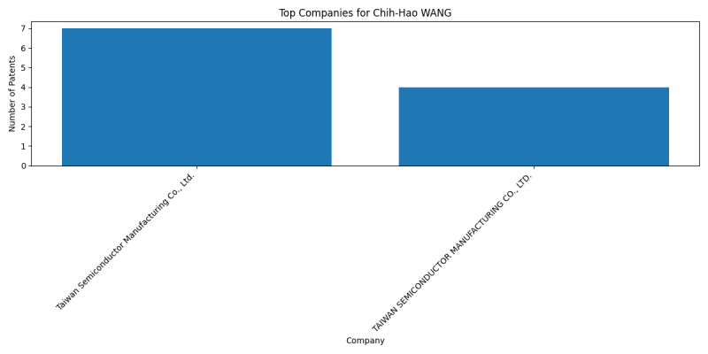
- Taiwan Semiconductor Manufacturing Company, Ltd.: 18 patents
- TAIWAN SEMICONDUCTOR MANUFACTURING COMPANY, LTD.: 16 patents
Collaborators
- Kuo-Cheng CHIANG (19 collaborations)
- Lin-Yu HUANG (10 collaborations)
- Huan-Chieh SU (9 collaborations)
- Shi-Ning JU (8 collaborations)
- Kuan-Lun CHENG (8 collaborations)
- Guan-Lin CHEN (6 collaborations)
- Shi Ning JU (6 collaborations)
- Kuan-Ting PAN (5 collaborations)
- Chun-Yuan CHEN (4 collaborations)
- Jung-Chien CHENG (4 collaborations)
- Li-Zhen YU (4 collaborations)
- Lo-Heng CHANG (4 collaborations)
- Jia-Ni YU (3 collaborations)
- Mao-Lin HUANG (3 collaborations)
- Lung-Kun CHU (3 collaborations)
- Chung-Wei HSU (3 collaborations)
- Chun-Fu LU (3 collaborations)
- Jia-Chuan YOU (3 collaborations)
- Chia-Hao CHANG (3 collaborations)
- Yu-Ming LIN (3 collaborations)
- Cheng-Chi CHUANG (3 collaborations)
- Yu-Xuan HUANG (3 collaborations)
- Tien-Lu LIN (2 collaborations)
- Meng-Huan JAO (2 collaborations)
- Yi-Ruei JHAN (2 collaborations)
- Ching-Wei TSAI (2 collaborations)
- Jung-Hung CHANG (2 collaborations)
- Sheng-Tsung WANG (2 collaborations)
- Wang-Chun HUANG (2 collaborations)
- Hou-Yu CHEN (2 collaborations)
- Bo-Rong LIN (2 collaborations)
- Jin CAI (1 collaborations)
- Shih-Chuan CHIU (1 collaborations)
- Pei-Yu WANG (1 collaborations)
- Cheng-Ting CHUNG (1 collaborations)
- Min CAO (1 collaborations)
- Pei-Hsun WANG (1 collaborations)
- Yun-Ju FAN (1 collaborations)
- Wei-Ting WANG (1 collaborations)
- Yi-Bo LIAO (1 collaborations)
- Yi-Hsun CHIU (1 collaborations)
- Hsiao-Han LIU (1 collaborations)
- Zhi-Chang LIN (1 collaborations)
- Shih-Cheng CHEN (1 collaborations)
- Chien Ning YAO (1 collaborations)
- Kuo-Cheng CHING (1 collaborations)
Subcategories
This category has the following 3 subcategories, out of 3 total.
Categories:
- Kuo-Cheng CHIANG
- Lin-Yu HUANG
- Huan-Chieh SU
- Shi-Ning JU
- Kuan-Lun CHENG
- Guan-Lin CHEN
- Shi Ning JU
- Kuan-Ting PAN
- Chun-Yuan CHEN
- Jung-Chien CHENG
- Li-Zhen YU
- Lo-Heng CHANG
- Jia-Ni YU
- Mao-Lin HUANG
- Lung-Kun CHU
- Chung-Wei HSU
- Chun-Fu LU
- Jia-Chuan YOU
- Chia-Hao CHANG
- Yu-Ming LIN
- Cheng-Chi CHUANG
- Yu-Xuan HUANG
- Tien-Lu LIN
- Meng-Huan JAO
- Yi-Ruei JHAN
- Ching-Wei TSAI
- Jung-Hung CHANG
- Sheng-Tsung WANG
- Wang-Chun HUANG
- Hou-Yu CHEN
- Bo-Rong LIN
- Jin CAI
- Shih-Chuan CHIU
- Pei-Yu WANG
- Cheng-Ting CHUNG
- Min CAO
- Pei-Hsun WANG
- Yun-Ju FAN
- Wei-Ting WANG
- Yi-Bo LIAO
- Yi-Hsun CHIU
- Hsiao-Han LIU
- Zhi-Chang LIN
- Shih-Cheng CHEN
- Chien Ning YAO
- Kuo-Cheng CHING
- Chih-Hao WANG
- Inventors
- Inventors filing patents with Taiwan Semiconductor Manufacturing Company, Ltd.
- Inventors filing patents with TAIWAN SEMICONDUCTOR MANUFACTURING COMPANY, LTD.


