Category:Sai-Hooi Yeong
Revision as of 06:48, 18 July 2024 by Wikipatents (talk | contribs) (Updating Category:Sai-Hooi_Yeong)
Contents
Sai-Hooi Yeong
Executive Summary
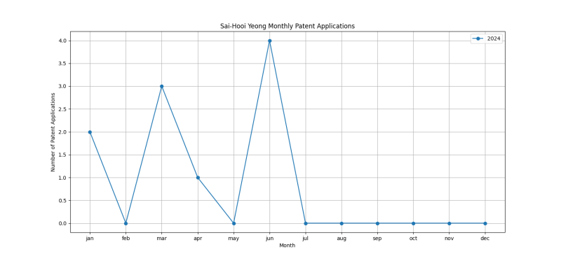
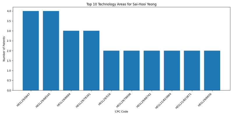
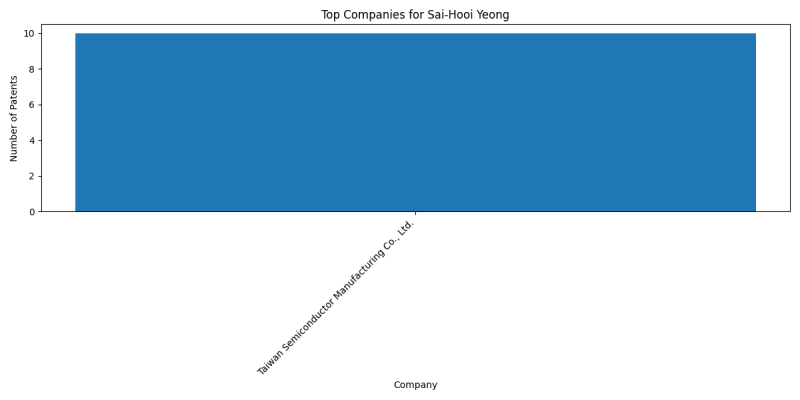
Sai-Hooi Yeong is an inventor who has filed 10 patents. Their primary areas of innovation include SEMICONDUCTOR DEVICES NOT COVERED BY CLASS (4 patents), {using a dummy, i.e. replacement gate in a process wherein at least a part of the final gate is self aligned to the dummy gate} (4 patents), SEMICONDUCTOR DEVICES NOT COVERED BY CLASS (3 patents), and they have worked with companies such as Taiwan Semiconductor Manufacturing Co., Ltd. (10 patents). Their most frequent collaborators include (5 collaborations), (4 collaborations), (3 collaborations).
Patent Filing Activity
Technology Areas
List of Technology Areas
- H01L29/0847 (SEMICONDUCTOR DEVICES NOT COVERED BY CLASS): 4 patents
- H01L29/66545 ({using a dummy, i.e. replacement gate in a process wherein at least a part of the final gate is self aligned to the dummy gate}): 4 patents
- H01L29/6684 (SEMICONDUCTOR DEVICES NOT COVERED BY CLASS): 3 patents
- H01L29/78391 (SEMICONDUCTOR DEVICES NOT COVERED BY CLASS): 3 patents
- H01L29/516 (SEMICONDUCTOR DEVICES NOT COVERED BY CLASS): 2 patents
- H01L29/78696 (SEMICONDUCTOR DEVICES NOT COVERED BY CLASS): 2 patents
- H01L29/66742 (SEMICONDUCTOR DEVICES NOT COVERED BY CLASS): 2 patents
- H01L21/823864 (to produce devices, e.g. integrated circuits, each consisting of a plurality of components): 2 patents
- H01L21/823871 (to produce devices, e.g. integrated circuits, each consisting of a plurality of components): 2 patents
- H01L29/6656 ({using self aligned silicidation, i.e. salicide (formation of conductive layers comprising silicides): 2 patents
- H01L29/165 (SEMICONDUCTOR DEVICES NOT COVERED BY CLASS): 2 patents
- H01L21/30604 (Chemical or electrical treatment, e.g. electrolytic etching (to form insulating layers): 2 patents
- H01L21/823821 (to produce devices, e.g. integrated circuits, each consisting of a plurality of components): 2 patents
- H01L27/0924 (SEMICONDUCTOR DEVICES NOT COVERED BY CLASS): 2 patents
- H01L29/66636 (SEMICONDUCTOR DEVICES NOT COVERED BY CLASS): 2 patents
- H01L21/823814 (to produce devices, e.g. integrated circuits, each consisting of a plurality of components): 2 patents
- H01L27/092 (SEMICONDUCTOR DEVICES NOT COVERED BY CLASS): 2 patents
- H01L29/66553 ({using self aligned silicidation, i.e. salicide (formation of conductive layers comprising silicides): 2 patents
- H01L21/823857 (to produce devices, e.g. integrated circuits, each consisting of a plurality of components): 2 patents
- H01L29/513 (SEMICONDUCTOR DEVICES NOT COVERED BY CLASS): 2 patents
- H10B51/20 (ELECTRONIC MEMORY DEVICES): 1 patents
- H01L23/5283 ({Geometry or} layout of the interconnection structure {(): 1 patents
- H10B51/30 (ELECTRONIC MEMORY DEVICES): 1 patents
- H01L29/7869 (SEMICONDUCTOR DEVICES NOT COVERED BY CLASS): 1 patents
- H01L29/0649 (SEMICONDUCTOR DEVICES NOT COVERED BY CLASS): 1 patents
- H01L21/764 (Making of isolation regions between components): 1 patents
- H01L21/7682 (Applying interconnections to be used for carrying current between separate components within a device {comprising conductors and dielectrics}): 1 patents
- H01L21/76841 (Applying interconnections to be used for carrying current between separate components within a device {comprising conductors and dielectrics}): 1 patents
- H01L21/76897 ({Formation of self-aligned vias or contact plugs, i.e. involving a lithographically uncritical step (self-aligned silicidation on field effect transistors): 1 patents
- H01L23/10 (SEMICONDUCTOR DEVICES NOT COVERED BY CLASS): 1 patents
- H01L29/6681 (SEMICONDUCTOR DEVICES NOT COVERED BY CLASS): 1 patents
- H01L29/66803 (SEMICONDUCTOR DEVICES NOT COVERED BY CLASS): 1 patents
- H01L21/225 (using diffusion into or out of a solid from or into a solid phase, e.g. a doped oxide layer {(): 1 patents
- H01L21/26526 (producing ion implantation): 1 patents
- H01L29/66818 (SEMICONDUCTOR DEVICES NOT COVERED BY CLASS): 1 patents
- H10B10/12 (ELECTRONIC MEMORY DEVICES): 1 patents
- H01L21/0273 ({characterised by the treatment of photoresist layers}): 1 patents
- H01L21/31111 ({by chemical means}): 1 patents
- H01L21/31144 ({using masks}): 1 patents
- H01L21/823418 (to produce devices, e.g. integrated circuits, each consisting of a plurality of components): 1 patents
- H01L21/823431 (to produce devices, e.g. integrated circuits, each consisting of a plurality of components): 1 patents
- H01L21/823437 (to produce devices, e.g. integrated circuits, each consisting of a plurality of components): 1 patents
- H10B10/18 (ELECTRONIC MEMORY DEVICES): 1 patents
- G11C8/08 (Word line control circuits, e.g. drivers, boosters, pull-up circuits, pull-down circuits, precharging circuits, for word lines): 1 patents
- G11C29/025 (STATIC STORES (semiconductor memory devices): 1 patents
- G11C29/12 (STATIC STORES (semiconductor memory devices): 1 patents
- G11C29/50 (STATIC STORES (semiconductor memory devices): 1 patents
- H01L21/8221 ({Three dimensional integrated circuits stacked in different levels}): 1 patents
- G11C2029/1202 (STATIC STORES (semiconductor memory devices): 1 patents
- H01L29/41733 (SEMICONDUCTOR DEVICES NOT COVERED BY CLASS): 1 patents
- H01L29/0673 (SEMICONDUCTOR DEVICES NOT COVERED BY CLASS): 1 patents
- H01L29/42392 (SEMICONDUCTOR DEVICES NOT COVERED BY CLASS): 1 patents
- H01L29/66439 (SEMICONDUCTOR DEVICES NOT COVERED BY CLASS): 1 patents
- H01L29/6653 ({using self aligned silicidation, i.e. salicide (formation of conductive layers comprising silicides): 1 patents
- H01L29/775 (SEMICONDUCTOR DEVICES NOT COVERED BY CLASS): 1 patents
- H01L29/7834 (SEMICONDUCTOR DEVICES NOT COVERED BY CLASS): 1 patents
- H01L21/3065 (Plasma etching; Reactive-ion etching): 1 patents
- H01L21/0206 ({during, before or after processing of insulating layers}): 1 patents
- H01L21/823828 (to produce devices, e.g. integrated circuits, each consisting of a plurality of components): 1 patents
- H01L29/42364 (SEMICONDUCTOR DEVICES NOT COVERED BY CLASS): 1 patents
- H01L29/517 (SEMICONDUCTOR DEVICES NOT COVERED BY CLASS): 1 patents
- H01L29/66795 (SEMICONDUCTOR DEVICES NOT COVERED BY CLASS): 1 patents
- H01L29/7851 (SEMICONDUCTOR DEVICES NOT COVERED BY CLASS): 1 patents
- H01L29/41775 (SEMICONDUCTOR DEVICES NOT COVERED BY CLASS): 1 patents
- H01L21/823456 (to produce devices, e.g. integrated circuits, each consisting of a plurality of components): 1 patents
- H01L21/823462 (to produce devices, e.g. integrated circuits, each consisting of a plurality of components): 1 patents
- H01L21/823475 (to produce devices, e.g. integrated circuits, each consisting of a plurality of components): 1 patents
- H01L27/088 (SEMICONDUCTOR DEVICES NOT COVERED BY CLASS): 1 patents
- H01L27/0922 (SEMICONDUCTOR DEVICES NOT COVERED BY CLASS): 1 patents
- H01L29/1079 (SEMICONDUCTOR DEVICES NOT COVERED BY CLASS): 1 patents
- H01L29/401 (SEMICONDUCTOR DEVICES NOT COVERED BY CLASS): 1 patents
- H01L29/66606 (SEMICONDUCTOR DEVICES NOT COVERED BY CLASS): 1 patents
- H01L29/66621 (SEMICONDUCTOR DEVICES NOT COVERED BY CLASS): 1 patents
Companies
List of Companies
- Taiwan Semiconductor Manufacturing Co., Ltd.: 10 patents
Collaborators
- Chi On Chui (5 collaborations)
- Meng-Han Lin (4 collaborations)
- Kai-Hsuan Lee (3 collaborations)
- Bo-Yu Lai (3 collaborations)
- Feng-Cheng Yang (3 collaborations)
- Yen-Ming Chen (3 collaborations)
- Sheng-Chen Wang (2 collaborations)
- Pei-Yu Wang (2 collaborations)
- Chia-En Huang (1 collaborations)
- Bo-Feng Young (1 collaborations)
- Yih-Ann Lin (1 collaborations)
- Ziwei Fang (1 collaborations)
- Chia-Ta Yu (1 collaborations)
- Cheng-Yu Yang (1 collaborations)
- Min Cao (1 collaborations)
- Ching-Wei Tsai (1 collaborations)
- Kuan-Lun Cheng (1 collaborations)
- Chih-Hao Wang (1 collaborations)
- Wen-Kai Lin (1 collaborations)
- Li Chun Te (1 collaborations)
- Tien-I Bao (1 collaborations)
- Wei-Ken Lin (1 collaborations)
Subcategories
This category has the following 8 subcategories, out of 8 total.
C
F
K
M
S
Y
Categories:
- Chi On Chui
- Meng-Han Lin
- Kai-Hsuan Lee
- Bo-Yu Lai
- Feng-Cheng Yang
- Yen-Ming Chen
- Sheng-Chen Wang
- Pei-Yu Wang
- Chia-En Huang
- Bo-Feng Young
- Yih-Ann Lin
- Ziwei Fang
- Chia-Ta Yu
- Cheng-Yu Yang
- Min Cao
- Ching-Wei Tsai
- Kuan-Lun Cheng
- Chih-Hao Wang
- Wen-Kai Lin
- Li Chun Te
- Tien-I Bao
- Wei-Ken Lin
- Sai-Hooi Yeong
- Inventors
- Inventors filing patents with Taiwan Semiconductor Manufacturing Co., Ltd.


