Category:Yee-Chia Yeo
Revision as of 01:38, 19 July 2024 by Wikipatents (talk | contribs) (Updating Category:Yee-Chia_Yeo)
Contents
Yee-Chia Yeo
Executive Summary
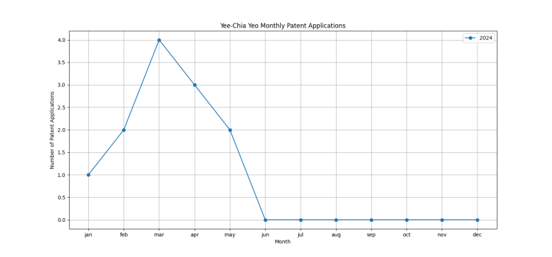
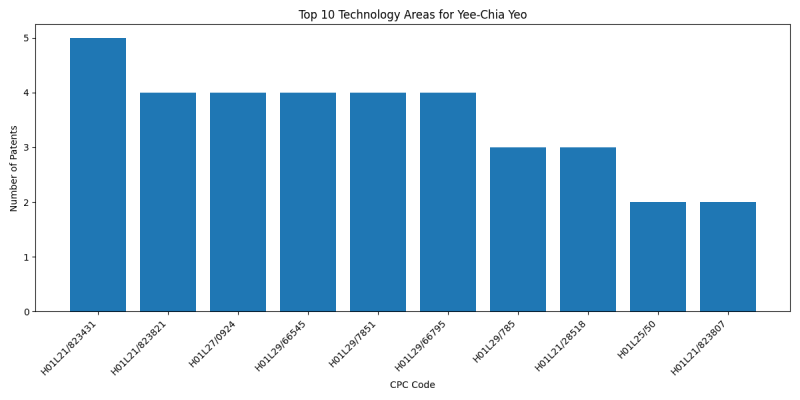
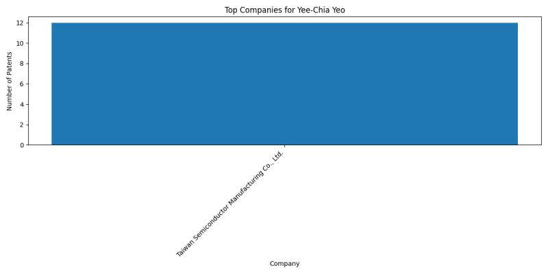
Yee-Chia Yeo is an inventor who has filed 12 patents. Their primary areas of innovation include to produce devices, e.g. integrated circuits, each consisting of a plurality of components (5 patents), to produce devices, e.g. integrated circuits, each consisting of a plurality of components (4 patents), SEMICONDUCTOR DEVICES NOT COVERED BY CLASS (4 patents), and they have worked with companies such as Taiwan Semiconductor Manufacturing Co., Ltd. (12 patents). Their most frequent collaborators include (10 collaborations), (5 collaborations), (3 collaborations).
Patent Filing Activity
Technology Areas
List of Technology Areas
- H01L21/823431 (to produce devices, e.g. integrated circuits, each consisting of a plurality of components): 5 patents
- H01L21/823821 (to produce devices, e.g. integrated circuits, each consisting of a plurality of components): 4 patents
- H01L27/0924 (SEMICONDUCTOR DEVICES NOT COVERED BY CLASS): 4 patents
- H01L29/66545 ({using a dummy, i.e. replacement gate in a process wherein at least a part of the final gate is self aligned to the dummy gate}): 4 patents
- H01L29/7851 (SEMICONDUCTOR DEVICES NOT COVERED BY CLASS): 4 patents
- H01L29/66795 (SEMICONDUCTOR DEVICES NOT COVERED BY CLASS): 4 patents
- H01L29/785 (SEMICONDUCTOR DEVICES NOT COVERED BY CLASS): 3 patents
- H01L21/28518 (from a gas or vapour, e.g. condensation): 3 patents
- H01L25/50 ({Multistep manufacturing processes of assemblies consisting of devices, each device being of a type provided for in group): 2 patents
- H01L21/823807 (to produce devices, e.g. integrated circuits, each consisting of a plurality of components): 2 patents
- H01L21/266 (using masks {(): 2 patents
- H01L21/823481 (to produce devices, e.g. integrated circuits, each consisting of a plurality of components): 2 patents
- H01L29/0649 (SEMICONDUCTOR DEVICES NOT COVERED BY CLASS): 2 patents
- H01L29/42392 (SEMICONDUCTOR DEVICES NOT COVERED BY CLASS): 2 patents
- H01L29/775 (SEMICONDUCTOR DEVICES NOT COVERED BY CLASS): 2 patents
- H01L21/31155 (Doping the insulating layers): 2 patents
- H01L21/823828 (to produce devices, e.g. integrated circuits, each consisting of a plurality of components): 2 patents
- H01L29/0847 (SEMICONDUCTOR DEVICES NOT COVERED BY CLASS): 2 patents
- H01L21/823418 (to produce devices, e.g. integrated circuits, each consisting of a plurality of components): 2 patents
- H01L24/83 (SEMICONDUCTOR DEVICES NOT COVERED BY CLASS): 1 patents
- H01L21/265 (producing ion implantation): 1 patents
- H01L21/6835 ({using temporarily an auxiliary support}): 1 patents
- H01L21/7806 ({involving the separation of the active layers from a substrate}): 1 patents
- H01L21/823892 (to produce devices, e.g. integrated circuits, each consisting of a plurality of components): 1 patents
- H01L27/0928 (SEMICONDUCTOR DEVICES NOT COVERED BY CLASS): 1 patents
- H01L21/76229 (Dielectric regions {, e.g. EPIC dielectric isolation, LOCOS; Trench refilling techniques, SOI technology, use of channel stoppers}): 1 patents
- H01L27/0886 (SEMICONDUCTOR DEVICES NOT COVERED BY CLASS): 1 patents
- H01L21/823412 (to produce devices, e.g. integrated circuits, each consisting of a plurality of components): 1 patents
- H01L29/0669 (SEMICONDUCTOR DEVICES NOT COVERED BY CLASS): 1 patents
- H01L29/66553 ({using self aligned silicidation, i.e. salicide (formation of conductive layers comprising silicides): 1 patents
- H01L29/78696 (SEMICONDUCTOR DEVICES NOT COVERED BY CLASS): 1 patents
- H01L21/764 (Making of isolation regions between components): 1 patents
- H01L21/7682 (Applying interconnections to be used for carrying current between separate components within a device {comprising conductors and dielectrics}): 1 patents
- H01L21/76825 ({by exposing the layer to particle radiation, e.g. ion implantation, irradiation with UV light or electrons etc. (plasma treatment): 1 patents
- H01L21/76831 ({in via holes or trenches, e.g. non-conductive sidewall liners}): 1 patents
- H01L21/76897 ({Formation of self-aligned vias or contact plugs, i.e. involving a lithographically uncritical step (self-aligned silicidation on field effect transistors): 1 patents
- H01L21/823864 (to produce devices, e.g. integrated circuits, each consisting of a plurality of components): 1 patents
- H01L21/823871 (to produce devices, e.g. integrated circuits, each consisting of a plurality of components): 1 patents
- H01L29/41725 (SEMICONDUCTOR DEVICES NOT COVERED BY CLASS): 1 patents
- H01L29/41766 (SEMICONDUCTOR DEVICES NOT COVERED BY CLASS): 1 patents
- H01L29/41791 (SEMICONDUCTOR DEVICES NOT COVERED BY CLASS): 1 patents
- H01L29/4991 (SEMICONDUCTOR DEVICES NOT COVERED BY CLASS): 1 patents
- H01L29/6653 ({using self aligned silicidation, i.e. salicide (formation of conductive layers comprising silicides): 1 patents
- H01L21/823468 (to produce devices, e.g. integrated circuits, each consisting of a plurality of components): 1 patents
- H01L21/681 (for positioning, orientation or alignment): 1 patents
- G06T1/0014 ({Image feed-back for automatic industrial control, e.g. robot with camera (robots): 1 patents
- G06T7/0004 ({Industrial image inspection}): 1 patents
- G06T7/73 (using feature-based methods): 1 patents
- H01L23/544 (Marks applied to semiconductor devices {or parts}, e.g. registration marks, {alignment structures, wafer maps (test patterns for characterising or monitoring manufacturing processes): 1 patents
- G06T2207/30148 (Subject of image; Context of image processing): 1 patents
- H01L2223/54493 (SEMICONDUCTOR DEVICES NOT COVERED BY CLASS): 1 patents
- H01L29/401 (SEMICONDUCTOR DEVICES NOT COVERED BY CLASS): 1 patents
- H01L21/0337 ({characterised by the process involved to create the mask, e.g. lift-off masks, sidewalls, or to modify the mask, e.g. pre-treatment, post-treatment}): 1 patents
- H01L29/456 (SEMICONDUCTOR DEVICES NOT COVERED BY CLASS): 1 patents
- H01L21/02532 (SEMICONDUCTOR DEVICES NOT COVERED BY CLASS): 1 patents
- H01L21/26506 (producing ion implantation): 1 patents
- H01L21/324 (SEMICONDUCTOR DEVICES NOT COVERED BY CLASS): 1 patents
- H01L21/76814 ({post-treatment or after-treatment, e.g. cleaning or removal of oxides on underlying conductors}): 1 patents
- H01L21/823814 (to produce devices, e.g. integrated circuits, each consisting of a plurality of components): 1 patents
- H01L29/161 (SEMICONDUCTOR DEVICES NOT COVERED BY CLASS): 1 patents
- H01L29/66507 ({providing different silicide thicknesses on the gate and on source or drain}): 1 patents
- H01L29/7845 (SEMICONDUCTOR DEVICES NOT COVERED BY CLASS): 1 patents
- H01L29/7848 (SEMICONDUCTOR DEVICES NOT COVERED BY CLASS): 1 patents
- H01L2029/7858 (SEMICONDUCTOR DEVICES NOT COVERED BY CLASS): 1 patents
- H01L21/568 (SEMICONDUCTOR DEVICES NOT COVERED BY CLASS): 1 patents
- H01L21/561 (SEMICONDUCTOR DEVICES NOT COVERED BY CLASS): 1 patents
- H01L25/0652 (SEMICONDUCTOR DEVICES NOT COVERED BY CLASS): 1 patents
- H01L29/66439 (SEMICONDUCTOR DEVICES NOT COVERED BY CLASS): 1 patents
- H01L29/0673 (SEMICONDUCTOR DEVICES NOT COVERED BY CLASS): 1 patents
Companies
List of Companies
- Taiwan Semiconductor Manufacturing Co., Ltd.: 12 patents
Collaborators
- Huicheng Chang (10 collaborations)
- Liang-Yin Chen (5 collaborations)
- Su-Hao Liu (3 collaborations)
- Jyh-Cherng Sheu (2 collaborations)
- Chen-Fong Tsai (2 collaborations)
- Yun Chen Teng (2 collaborations)
- Han-De Chen (2 collaborations)
- Wen-Yen Chen (2 collaborations)
- Tsai-Yu Huang (2 collaborations)
- Jhih-Yong Han (1 collaborations)
- Yi-Ting Wu (1 collaborations)
- Szu-Ying Chen (1 collaborations)
- Sen-Hong Syue (1 collaborations)
- Yu-Chang Lin (1 collaborations)
- Chun-Feng Nieh (1 collaborations)
- Kuo-Ju Chen (1 collaborations)
- Kai-Hsuan Lee (1 collaborations)
- I-Hsieh Wong (1 collaborations)
- Cheng-Yu Yang (1 collaborations)
- Syun-Ming Jang (1 collaborations)
- Meng-Han Chou (1 collaborations)
- Chih-Yun Chin (1 collaborations)
- Yen-Ru Lee (1 collaborations)
- Chien-Chang Su (1 collaborations)
- Yan-Ting Lin (1 collaborations)
- Chien-Wei Lee (1 collaborations)
- Bang-Ting Yan (1 collaborations)
- Heng-Wen Ting (1 collaborations)
- Chii-Horng Li (1 collaborations)
- Chia-Cheng Chen (1 collaborations)
- Chih-Kai Yang (1 collaborations)
- Po-Kang Ho (1 collaborations)
- Tsan-Chun Wang (1 collaborations)
- Li-Heng Chen (1 collaborations)
- Li-Ting Wang (1 collaborations)
- Ying-Lang Wang (1 collaborations)
- Wei-Ting Chien (1 collaborations)
Subcategories
This category has the following 2 subcategories, out of 2 total.
Categories:
- Huicheng Chang
- Liang-Yin Chen
- Su-Hao Liu
- Jyh-Cherng Sheu
- Chen-Fong Tsai
- Yun Chen Teng
- Han-De Chen
- Wen-Yen Chen
- Tsai-Yu Huang
- Jhih-Yong Han
- Yi-Ting Wu
- Szu-Ying Chen
- Sen-Hong Syue
- Yu-Chang Lin
- Chun-Feng Nieh
- Kuo-Ju Chen
- Kai-Hsuan Lee
- I-Hsieh Wong
- Cheng-Yu Yang
- Syun-Ming Jang
- Meng-Han Chou
- Chih-Yun Chin
- Yen-Ru Lee
- Chien-Chang Su
- Yan-Ting Lin
- Chien-Wei Lee
- Bang-Ting Yan
- Heng-Wen Ting
- Chii-Horng Li
- Chia-Cheng Chen
- Chih-Kai Yang
- Po-Kang Ho
- Tsan-Chun Wang
- Li-Heng Chen
- Li-Ting Wang
- Ying-Lang Wang
- Wei-Ting Chien
- Yee-Chia Yeo
- Inventors
- Inventors filing patents with Taiwan Semiconductor Manufacturing Co., Ltd.


