Category:Toshinari SASAKI
Revision as of 12:54, 18 July 2024 by Wikipatents (talk | contribs) (Updating Category:Toshinari_SASAKI)
Contents
Toshinari SASAKI
Executive Summary
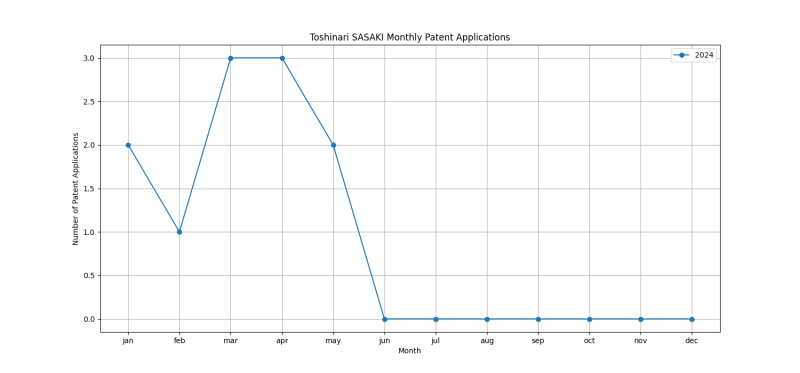
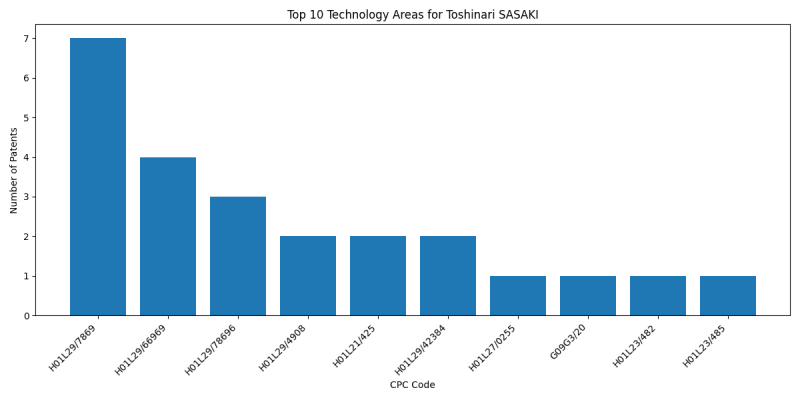
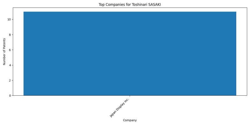
Toshinari SASAKI is an inventor who has filed 11 patents. Their primary areas of innovation include SEMICONDUCTOR DEVICES NOT COVERED BY CLASS (7 patents), {of devices having semiconductor bodies not comprising group 14 or group 13/15 materials (comprising selenium or tellurium in uncombined form other than as impurities in semiconductor bodies of other materials, comprising cuprous oxide or cuprous iodide (4 patents), SEMICONDUCTOR DEVICES NOT COVERED BY CLASS (3 patents), and they have worked with companies such as Japan Display Inc. (11 patents). Their most frequent collaborators include (10 collaborations), (10 collaborations), (9 collaborations).
Patent Filing Activity
Technology Areas
List of Technology Areas
- H01L29/7869 (SEMICONDUCTOR DEVICES NOT COVERED BY CLASS): 7 patents
- H01L29/66969 ({of devices having semiconductor bodies not comprising group 14 or group 13/15 materials (comprising selenium or tellurium in uncombined form other than as impurities in semiconductor bodies of other materials, comprising cuprous oxide or cuprous iodide): 4 patents
- H01L29/78696 (SEMICONDUCTOR DEVICES NOT COVERED BY CLASS): 3 patents
- H01L29/4908 (SEMICONDUCTOR DEVICES NOT COVERED BY CLASS): 2 patents
- H01L21/425 (producing ion implantation): 2 patents
- H01L29/42384 (SEMICONDUCTOR DEVICES NOT COVERED BY CLASS): 2 patents
- H01L27/0255 ({using diodes as protective elements}): 1 patents
- G09G3/20 (for presentation of an assembly of a number of characters, e.g. a page, by composing the assembly by combination of individual elements arranged in a matrix {no fixed position being assigned to or needed to be assigned to the individual characters or partial characters}): 1 patents
- H01L23/482 (consisting of lead-in layers inseparably applied to the semiconductor body {(electrodes): 1 patents
- H01L23/485 (consisting of layered constructions comprising conductive layers and insulating layers, e.g. planar contacts {(): 1 patents
- H01L29/42376 (SEMICONDUCTOR DEVICES NOT COVERED BY CLASS): 1 patents
- H01L29/45 (SEMICONDUCTOR DEVICES NOT COVERED BY CLASS): 1 patents
- H01L29/7391 (SEMICONDUCTOR DEVICES NOT COVERED BY CLASS): 1 patents
- H01L29/861 (SEMICONDUCTOR DEVICES NOT COVERED BY CLASS): 1 patents
- H01L29/872 (SEMICONDUCTOR DEVICES NOT COVERED BY CLASS): 1 patents
- G09G2300/0885 (ARRANGEMENTS OR CIRCUITS FOR CONTROL OF INDICATING DEVICES USING STATIC MEANS TO PRESENT VARIABLE INFORMATION (arrangements for transferring data between digital computers and displays): 1 patents
- G09G2330/04 (ARRANGEMENTS OR CIRCUITS FOR CONTROL OF INDICATING DEVICES USING STATIC MEANS TO PRESENT VARIABLE INFORMATION (arrangements for transferring data between digital computers and displays): 1 patents
- G09G2330/08 (ARRANGEMENTS OR CIRCUITS FOR CONTROL OF INDICATING DEVICES USING STATIC MEANS TO PRESENT VARIABLE INFORMATION (arrangements for transferring data between digital computers and displays): 1 patents
- H01L29/0692 (SEMICONDUCTOR DEVICES NOT COVERED BY CLASS): 1 patents
- H01L21/02667 (SEMICONDUCTOR DEVICES NOT COVERED BY CLASS): 1 patents
- H01L29/04 (SEMICONDUCTOR DEVICES NOT COVERED BY CLASS): 1 patents
- H01L21/02595 (SEMICONDUCTOR DEVICES NOT COVERED BY CLASS): 1 patents
- H01L21/02609 (SEMICONDUCTOR DEVICES NOT COVERED BY CLASS): 1 patents
- H01L21/02554 (SEMICONDUCTOR DEVICES NOT COVERED BY CLASS): 1 patents
- H01L21/02129 ({the material being boron or phosphorus doped silicon oxides, e.g. BPSG, BSG or PSG}): 1 patents
- H01L29/401 (SEMICONDUCTOR DEVICES NOT COVERED BY CLASS): 1 patents
- H10K59/131 (ORGANIC ELECTRIC SOLID-STATE DEVICES): 1 patents
- H10K59/1213 (ORGANIC ELECTRIC SOLID-STATE DEVICES): 1 patents
- G02F1/136227 (based on liquid crystals, e.g. single liquid crystal display cells): 1 patents
- G02F1/136286 (based on liquid crystals, e.g. single liquid crystal display cells): 1 patents
- G02F1/13685 (based on liquid crystals, e.g. single liquid crystal display cells): 1 patents
- G06F3/044 (by capacitive means): 1 patents
- H01L29/0603 (SEMICONDUCTOR DEVICES NOT COVERED BY CLASS): 1 patents
- H01L21/02565 (SEMICONDUCTOR DEVICES NOT COVERED BY CLASS): 1 patents
- H01L21/02631 (SEMICONDUCTOR DEVICES NOT COVERED BY CLASS): 1 patents
- H01L21/47576 (Organic layers, e.g. photoresist (): 1 patents
- H01L29/78633 (SEMICONDUCTOR DEVICES NOT COVERED BY CLASS): 1 patents
- H01L2029/42388 (SEMICONDUCTOR DEVICES NOT COVERED BY CLASS): 1 patents
Companies
List of Companies
- Japan Display Inc.: 11 patents
Collaborators
- Hajime WATAKABE (10 collaborations)
- Masashi TSUBUKU (10 collaborations)
- Takaya TAMARU (9 collaborations)
- Akihiro HANADA (2 collaborations)
- Marina MOCHIZUKI (1 collaborations)
- Ryo ONODERA (1 collaborations)
- Takay TAMARU (1 collaborations)
Subcategories
This category has the following 5 subcategories, out of 5 total.


