Difference between revisions of "Category:Koichi IGETA"
Jump to navigation
Jump to search
Wikipatents (talk | contribs) (Updating Category:Koichi_IGETA) |
Wikipatents (talk | contribs) (Updating Category:Koichi_IGETA) |
||
| Line 2: | Line 2: | ||
=== Executive Summary === | === Executive Summary === | ||
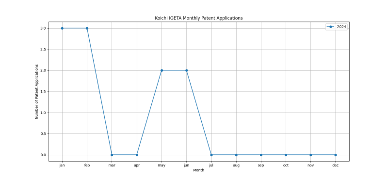
| − | Koichi IGETA is an inventor who has filed 10 patents. Their primary areas of innovation include | + | Koichi IGETA is an inventor who has filed 10 patents. Their primary areas of innovation include Constructional arrangements; Operation of liquid crystal cells; Circuit arrangements (arrangements or circuits for control of liquid crystal elements in a matrix, not structurally associated with these elements (4 patents), OPTICAL ELEMENTS, SYSTEMS OR APPARATUS (2 patents), based on polymer dispersed liquid crystals, e.g. microencapsulated liquid crystals (2 patents), and they have worked with companies such as Japan Display Inc. (10 patents). Their most frequent collaborators include [[Category:Shinichiro OKA|Shinichiro OKA]] (7 collaborations), [[Category:Yasushi TOMIOKA|Yasushi TOMIOKA]] (5 collaborations), [[Category:Junji KOBASHI|Junji KOBASHI]] (5 collaborations). |
=== Patent Filing Activity === | === Patent Filing Activity === | ||
| Line 11: | Line 11: | ||
==== List of Technology Areas ==== | ==== List of Technology Areas ==== | ||
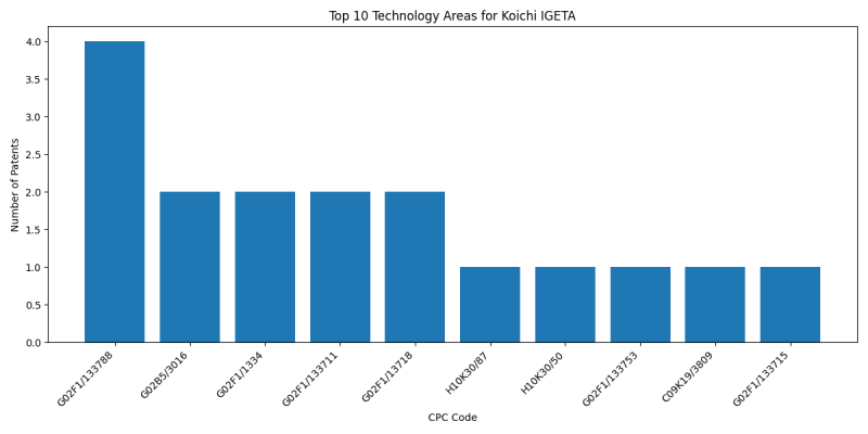
| − | * [[:Category:CPC_G02F1/133788|G02F1/133788]] ( | + | * [[:Category:CPC_G02F1/133788|G02F1/133788]] (Constructional arrangements; Operation of liquid crystal cells; Circuit arrangements (arrangements or circuits for control of liquid crystal elements in a matrix, not structurally associated with these elements): 4 patents |
| − | * [[:Category:CPC_G02B5/3016|G02B5/3016]] ( | + | * [[:Category:CPC_G02B5/3016|G02B5/3016]] (OPTICAL ELEMENTS, SYSTEMS OR APPARATUS): 2 patents |
| − | * [[:Category:CPC_G02F1/1334|G02F1/1334]] ( | + | * [[:Category:CPC_G02F1/1334|G02F1/1334]] (based on polymer dispersed liquid crystals, e.g. microencapsulated liquid crystals): 2 patents |
| − | * [[:Category:CPC_G02F1/133711|G02F1/133711]] ( | + | * [[:Category:CPC_G02F1/133711|G02F1/133711]] (Constructional arrangements; Operation of liquid crystal cells; Circuit arrangements (arrangements or circuits for control of liquid crystal elements in a matrix, not structurally associated with these elements): 2 patents |
| − | * [[:Category:CPC_G02F1/13718|G02F1/13718]] ( | + | * [[:Category:CPC_G02F1/13718|G02F1/13718]] (based on liquid crystals, e.g. single liquid crystal display cells): 2 patents |
| − | * [[:Category:CPC_H10K30/87|H10K30/87]] ( | + | * [[:Category:CPC_H10K30/87|H10K30/87]] (ORGANIC ELECTRIC SOLID-STATE DEVICES): 1 patents |
| − | * [[:Category:CPC_H10K30/50|H10K30/50]] ( | + | * [[:Category:CPC_H10K30/50|H10K30/50]] (ORGANIC ELECTRIC SOLID-STATE DEVICES): 1 patents |
| − | * [[:Category:CPC_G02F1/133753|G02F1/133753]] ( | + | * [[:Category:CPC_G02F1/133753|G02F1/133753]] (Constructional arrangements; Operation of liquid crystal cells; Circuit arrangements (arrangements or circuits for control of liquid crystal elements in a matrix, not structurally associated with these elements): 1 patents |
| − | * [[:Category:CPC_C09K19/3809|C09K19/3809]] ( | + | * [[:Category:CPC_C09K19/3809|C09K19/3809]] (Polymers): 1 patents |
| − | * [[:Category:CPC_G02F1/133715|G02F1/133715]] ( | + | * [[:Category:CPC_G02F1/133715|G02F1/133715]] (Constructional arrangements; Operation of liquid crystal cells; Circuit arrangements (arrangements or circuits for control of liquid crystal elements in a matrix, not structurally associated with these elements): 1 patents |
| − | * [[:Category:CPC_C09K19/542|C09K19/542]] ( | + | * [[:Category:CPC_C09K19/542|C09K19/542]] (MATERIALS FOR MISCELLANEOUS APPLICATIONS, NOT PROVIDED FOR ELSEWHERE): 1 patents |
| − | * [[:Category:CPC_C09K2019/546|C09K2019/546]] ( | + | * [[:Category:CPC_C09K2019/546|C09K2019/546]] (MATERIALS FOR MISCELLANEOUS APPLICATIONS, NOT PROVIDED FOR ELSEWHERE): 1 patents |
| − | * [[:Category:CPC_C09K2323/025|C09K2323/025]] ( | + | * [[:Category:CPC_C09K2323/025|C09K2323/025]] (MATERIALS FOR MISCELLANEOUS APPLICATIONS, NOT PROVIDED FOR ELSEWHERE): 1 patents |
| − | * [[:Category:CPC_G02B6/2726|G02B6/2726]] ( | + | * [[:Category:CPC_G02B6/2726|G02B6/2726]] (with polarisation selective and adjusting means): 1 patents |
| − | * [[:Category:CPC_G02F1/1347|G02F1/1347]] ( | + | * [[:Category:CPC_G02F1/1347|G02F1/1347]] (Arrangement of liquid crystal layers or cells in which the final condition of one light beam is achieved by the addition of the effects of two or more layers or cells): 1 patents |
| − | * [[:Category:CPC_G02F1/011|G02F1/011]] ( | + | * [[:Category:CPC_G02F1/011|G02F1/011]] ({in optical waveguides, not otherwise provided for in this subclass}): 1 patents |
| − | * [[:Category:CPC_G02F2201/50|G02F2201/50]] ( | + | * [[:Category:CPC_G02F2201/50|G02F2201/50]] (OPTICAL DEVICES OR ARRANGEMENTS FOR THE CONTROL OF LIGHT BY MODIFICATION OF THE OPTICAL PROPERTIES OF THE MEDIA OF THE ELEMENTS INVOLVED THEREIN; NON-LINEAR OPTICS; FREQUENCY-CHANGING OF LIGHT; OPTICAL LOGIC ELEMENTS; OPTICAL ANALOGUE/DIGITAL CONVERTERS): 1 patents |
| − | * [[:Category:CPC_G02F1/133761|G02F1/133761]] ( | + | * [[:Category:CPC_G02F1/133761|G02F1/133761]] (Constructional arrangements; Operation of liquid crystal cells; Circuit arrangements (arrangements or circuits for control of liquid crystal elements in a matrix, not structurally associated with these elements): 1 patents |
| − | * [[:Category:CPC_G02F1/133757|G02F1/133757]] ( | + | * [[:Category:CPC_G02F1/133757|G02F1/133757]] (Constructional arrangements; Operation of liquid crystal cells; Circuit arrangements (arrangements or circuits for control of liquid crystal elements in a matrix, not structurally associated with these elements): 1 patents |
| − | * [[:Category:CPC_G02F1/133365|G02F1/133365]] ( | + | * [[:Category:CPC_G02F1/133365|G02F1/133365]] ({Cells in which the active layer comprises a liquid crystalline polymer}): 1 patents |
| − | * [[:Category:CPC_G02F1/133536|G02F1/133536]] ( | + | * [[:Category:CPC_G02F1/133536|G02F1/133536]] (Structural association of cells with optical devices, e.g. polarisers or reflectors): 1 patents |
| − | * [[:Category:CPC_G02F1/133726|G02F1/133726]] ( | + | * [[:Category:CPC_G02F1/133726|G02F1/133726]] (Constructional arrangements; Operation of liquid crystal cells; Circuit arrangements (arrangements or circuits for control of liquid crystal elements in a matrix, not structurally associated with these elements): 1 patents |
| − | * [[:Category:CPC_G02F1/13478|G02F1/13478]] ( | + | * [[:Category:CPC_G02F1/13478|G02F1/13478]] (Arrangement of liquid crystal layers or cells in which the final condition of one light beam is achieved by the addition of the effects of two or more layers or cells): 1 patents |
| − | * [[:Category:CPC_H01L31/054|H01L31/054]] ( | + | * [[:Category:CPC_H01L31/054|H01L31/054]] (Optical elements directly associated or integrated with the PV cell, e.g. light-reflecting means or light-concentrating means): 1 patents |
| − | * [[:Category:CPC_G02F1/1339|G02F1/1339]] ( | + | * [[:Category:CPC_G02F1/1339|G02F1/1339]] (Constructional arrangements; Operation of liquid crystal cells; Circuit arrangements (arrangements or circuits for control of liquid crystal elements in a matrix, not structurally associated with these elements): 1 patents |
| − | * [[:Category:CPC_G02F1/136286|G02F1/136286]] ( | + | * [[:Category:CPC_G02F1/136286|G02F1/136286]] (based on liquid crystals, e.g. single liquid crystal display cells): 1 patents |
| − | * [[:Category:CPC_G02F1/133305|G02F1/133305]] ( | + | * [[:Category:CPC_G02F1/133305|G02F1/133305]] (Constructional arrangements; Operation of liquid crystal cells; Circuit arrangements (arrangements or circuits for control of liquid crystal elements in a matrix, not structurally associated with these elements): 1 patents |
=== Companies === | === Companies === | ||
Latest revision as of 12:55, 18 July 2024
Contents
Koichi IGETA
Executive Summary
Koichi IGETA is an inventor who has filed 10 patents. Their primary areas of innovation include Constructional arrangements; Operation of liquid crystal cells; Circuit arrangements (arrangements or circuits for control of liquid crystal elements in a matrix, not structurally associated with these elements (4 patents), OPTICAL ELEMENTS, SYSTEMS OR APPARATUS (2 patents), based on polymer dispersed liquid crystals, e.g. microencapsulated liquid crystals (2 patents), and they have worked with companies such as Japan Display Inc. (10 patents). Their most frequent collaborators include (7 collaborations), (5 collaborations), (5 collaborations).
Patent Filing Activity
Technology Areas
List of Technology Areas
- G02F1/133788 (Constructional arrangements; Operation of liquid crystal cells; Circuit arrangements (arrangements or circuits for control of liquid crystal elements in a matrix, not structurally associated with these elements): 4 patents
- G02B5/3016 (OPTICAL ELEMENTS, SYSTEMS OR APPARATUS): 2 patents
- G02F1/1334 (based on polymer dispersed liquid crystals, e.g. microencapsulated liquid crystals): 2 patents
- G02F1/133711 (Constructional arrangements; Operation of liquid crystal cells; Circuit arrangements (arrangements or circuits for control of liquid crystal elements in a matrix, not structurally associated with these elements): 2 patents
- G02F1/13718 (based on liquid crystals, e.g. single liquid crystal display cells): 2 patents
- H10K30/87 (ORGANIC ELECTRIC SOLID-STATE DEVICES): 1 patents
- H10K30/50 (ORGANIC ELECTRIC SOLID-STATE DEVICES): 1 patents
- G02F1/133753 (Constructional arrangements; Operation of liquid crystal cells; Circuit arrangements (arrangements or circuits for control of liquid crystal elements in a matrix, not structurally associated with these elements): 1 patents
- C09K19/3809 (Polymers): 1 patents
- G02F1/133715 (Constructional arrangements; Operation of liquid crystal cells; Circuit arrangements (arrangements or circuits for control of liquid crystal elements in a matrix, not structurally associated with these elements): 1 patents
- C09K19/542 (MATERIALS FOR MISCELLANEOUS APPLICATIONS, NOT PROVIDED FOR ELSEWHERE): 1 patents
- C09K2019/546 (MATERIALS FOR MISCELLANEOUS APPLICATIONS, NOT PROVIDED FOR ELSEWHERE): 1 patents
- C09K2323/025 (MATERIALS FOR MISCELLANEOUS APPLICATIONS, NOT PROVIDED FOR ELSEWHERE): 1 patents
- G02B6/2726 (with polarisation selective and adjusting means): 1 patents
- G02F1/1347 (Arrangement of liquid crystal layers or cells in which the final condition of one light beam is achieved by the addition of the effects of two or more layers or cells): 1 patents
- G02F1/011 ({in optical waveguides, not otherwise provided for in this subclass}): 1 patents
- G02F2201/50 (OPTICAL DEVICES OR ARRANGEMENTS FOR THE CONTROL OF LIGHT BY MODIFICATION OF THE OPTICAL PROPERTIES OF THE MEDIA OF THE ELEMENTS INVOLVED THEREIN; NON-LINEAR OPTICS; FREQUENCY-CHANGING OF LIGHT; OPTICAL LOGIC ELEMENTS; OPTICAL ANALOGUE/DIGITAL CONVERTERS): 1 patents
- G02F1/133761 (Constructional arrangements; Operation of liquid crystal cells; Circuit arrangements (arrangements or circuits for control of liquid crystal elements in a matrix, not structurally associated with these elements): 1 patents
- G02F1/133757 (Constructional arrangements; Operation of liquid crystal cells; Circuit arrangements (arrangements or circuits for control of liquid crystal elements in a matrix, not structurally associated with these elements): 1 patents
- G02F1/133365 ({Cells in which the active layer comprises a liquid crystalline polymer}): 1 patents
- G02F1/133536 (Structural association of cells with optical devices, e.g. polarisers or reflectors): 1 patents
- G02F1/133726 (Constructional arrangements; Operation of liquid crystal cells; Circuit arrangements (arrangements or circuits for control of liquid crystal elements in a matrix, not structurally associated with these elements): 1 patents
- G02F1/13478 (Arrangement of liquid crystal layers or cells in which the final condition of one light beam is achieved by the addition of the effects of two or more layers or cells): 1 patents
- H01L31/054 (Optical elements directly associated or integrated with the PV cell, e.g. light-reflecting means or light-concentrating means): 1 patents
- G02F1/1339 (Constructional arrangements; Operation of liquid crystal cells; Circuit arrangements (arrangements or circuits for control of liquid crystal elements in a matrix, not structurally associated with these elements): 1 patents
- G02F1/136286 (based on liquid crystals, e.g. single liquid crystal display cells): 1 patents
- G02F1/133305 (Constructional arrangements; Operation of liquid crystal cells; Circuit arrangements (arrangements or circuits for control of liquid crystal elements in a matrix, not structurally associated with these elements): 1 patents
Companies
List of Companies
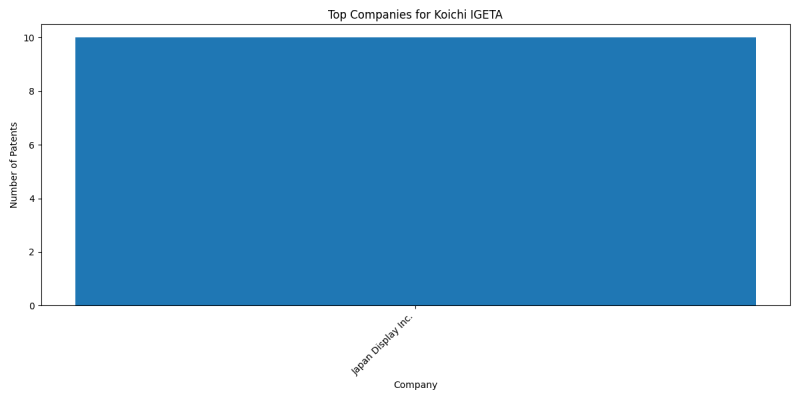
- Japan Display Inc.: 10 patents
Collaborators
- Shinichiro OKA (7 collaborations)
- Yasushi TOMIOKA (5 collaborations)
- Junji KOBASHI (5 collaborations)
- Hiroyuki YOSHIDA (3 collaborations)
- Hiroumi KINJO (2 collaborations)
- Ayaka HIGUCHI (2 collaborations)
- Kentaro OKUYAMA (2 collaborations)
- Yasuyuki YAMADA (1 collaborations)
- Koji KITAMURA (1 collaborations)
- Tenfu NAKAMURA (1 collaborations)
Subcategories
This category has the following 5 subcategories, out of 5 total.


