Difference between revisions of "Category:Takumi SANO"
Jump to navigation
Jump to search
Wikipatents (talk | contribs) (Updating Category:Takumi_SANO) |
Wikipatents (talk | contribs) (Updating Category:Takumi_SANO) |
||
| Line 2: | Line 2: | ||
=== Executive Summary === | === Executive Summary === | ||
| − | Takumi SANO is an inventor who has filed | + | Takumi SANO is an inventor who has filed 12 patents. Their primary areas of innovation include PRINTED CIRCUITS; CASINGS OR CONSTRUCTIONAL DETAILS OF ELECTRIC APPARATUS; MANUFACTURE OF ASSEMBLAGES OF ELECTRICAL COMPONENTS (5 patents), PRINTED CIRCUITS; CASINGS OR CONSTRUCTIONAL DETAILS OF ELECTRIC APPARATUS; MANUFACTURE OF ASSEMBLAGES OF ELECTRICAL COMPONENTS (4 patents), {using a single layer of sensing electrodes} (3 patents), and they have worked with companies such as Japan Display Inc. (12 patents). Their most frequent collaborators include [[Category:Masatomo HISHINUMA|Masatomo HISHINUMA]] (6 collaborations), [[Category:Yasushi TOMIOKA|Yasushi TOMIOKA]] (2 collaborations), [[Category:Akio MURAYAMA|Akio MURAYAMA]] (2 collaborations). |
=== Patent Filing Activity === | === Patent Filing Activity === | ||
| Line 11: | Line 11: | ||
==== List of Technology Areas ==== | ==== List of Technology Areas ==== | ||
| − | * [[:Category:CPC_H05K1/0283|H05K1/0283]] ( | + | * [[:Category:CPC_H05K1/0283|H05K1/0283]] (PRINTED CIRCUITS; CASINGS OR CONSTRUCTIONAL DETAILS OF ELECTRIC APPARATUS; MANUFACTURE OF ASSEMBLAGES OF ELECTRICAL COMPONENTS): 5 patents |
| − | * [[:Category:CPC_H05K2201/10151|H05K2201/10151]] ( | + | * [[:Category:CPC_H05K2201/10151|H05K2201/10151]] (PRINTED CIRCUITS; CASINGS OR CONSTRUCTIONAL DETAILS OF ELECTRIC APPARATUS; MANUFACTURE OF ASSEMBLAGES OF ELECTRICAL COMPONENTS): 4 patents |
| − | * [[:Category:CPC_G06F3/0443|G06F3/0443]] ( | + | * [[:Category:CPC_G06F3/0443|G06F3/0443]] ({using a single layer of sensing electrodes}): 3 patents |
| − | * [[:Category:CPC_G06F2203/04102|G06F2203/04102]] ( | + | * [[:Category:CPC_G06F2203/04102|G06F2203/04102]] (ELECTRIC DIGITAL DATA PROCESSING (computer systems based on specific computational models): 2 patents |
| − | * [[:Category:CPC_H05K1/0269|H05K1/0269]] ( | + | * [[:Category:CPC_H05K1/0269|H05K1/0269]] ({Spark gaps}): 1 patents |
| − | * [[:Category:CPC_H05K2201/09263|H05K2201/09263]] ( | + | * [[:Category:CPC_H05K2201/09263|H05K2201/09263]] (PRINTED CIRCUITS; CASINGS OR CONSTRUCTIONAL DETAILS OF ELECTRIC APPARATUS; MANUFACTURE OF ASSEMBLAGES OF ELECTRICAL COMPONENTS): 1 patents |
| − | * [[:Category:CPC_H05K1/032|H05K1/032]] ( | + | * [[:Category:CPC_H05K1/032|H05K1/032]] (Use of materials for the substrate): 1 patents |
| − | * [[:Category:CPC_H05K1/0306|H05K1/0306]] ( | + | * [[:Category:CPC_H05K1/0306|H05K1/0306]] (Use of materials for the substrate): 1 patents |
| − | * [[:Category:CPC_H05K1/118|H05K1/118]] ( | + | * [[:Category:CPC_H05K1/118|H05K1/118]] (PRINTED CIRCUITS; CASINGS OR CONSTRUCTIONAL DETAILS OF ELECTRIC APPARATUS; MANUFACTURE OF ASSEMBLAGES OF ELECTRICAL COMPONENTS): 1 patents |
| − | * [[:Category:CPC_H05K3/103|H05K3/103]] ( | + | * [[:Category:CPC_H05K3/103|H05K3/103]] (PRINTED CIRCUITS; CASINGS OR CONSTRUCTIONAL DETAILS OF ELECTRIC APPARATUS; MANUFACTURE OF ASSEMBLAGES OF ELECTRICAL COMPONENTS): 1 patents |
| − | * [[:Category:CPC_H05K2201/10106|H05K2201/10106]] ( | + | * [[:Category:CPC_H05K2201/10106|H05K2201/10106]] (PRINTED CIRCUITS; CASINGS OR CONSTRUCTIONAL DETAILS OF ELECTRIC APPARATUS; MANUFACTURE OF ASSEMBLAGES OF ELECTRICAL COMPONENTS): 1 patents |
| − | * [[:Category:CPC_G06F3/04146|G06F3/04146]] ( | + | * [[:Category:CPC_G06F3/04146|G06F3/04146]] ({using pressure sensitive conductive elements delivering a boolean signal and located between crossing sensing lines, e.g. located between X and Y sensing line layers}): 1 patents |
| − | * [[:Category:CPC_G01L1/205|G01L1/205]] ( | + | * [[:Category:CPC_G01L1/205|G01L1/205]] (MEASURING FORCE, STRESS, TORQUE, WORK, MECHANICAL POWER, MECHANICAL EFFICIENCY, OR FLUID PRESSURE (weighing): 1 patents |
| − | * [[:Category:CPC_G06F3/0412|G06F3/0412]] ( | + | * [[:Category:CPC_G06F3/0412|G06F3/0412]] ({Digitisers structurally integrated in a display}): 1 patents |
| − | * [[:Category:CPC_G06F2203/04105|G06F2203/04105]] ( | + | * [[:Category:CPC_G06F2203/04105|G06F2203/04105]] (ELECTRIC DIGITAL DATA PROCESSING (computer systems based on specific computational models): 1 patents |
| − | * [[:Category:CPC_G06F3/044|G06F3/044]] ( | + | * [[:Category:CPC_G06F3/044|G06F3/044]] (by capacitive means): 1 patents |
| − | * [[:Category:CPC_G06F2203/04108|G06F2203/04108]] ( | + | * [[:Category:CPC_G06F2203/04108|G06F2203/04108]] (ELECTRIC DIGITAL DATA PROCESSING (computer systems based on specific computational models): 1 patents |
| − | * [[:Category:CPC_G06F3/04166|G06F3/04166]] ( | + | * [[:Category:CPC_G06F3/04166|G06F3/04166]] ({Details of scanning methods, e.g. sampling time, grouping of sub areas or time sharing with display driving (Synchronisation with the driving of the display or the backlighting unit to avoid interferences generated internally): 1 patents |
| − | * [[:Category:CPC_G06F3/0446|G06F3/0446]] ( | + | * [[:Category:CPC_G06F3/0446|G06F3/0446]] ({using a grid-like structure of electrodes in at least two directions, e.g. using row and column electrodes}): 1 patents |
| + | * [[:Category:CPC_H01L23/5386|H01L23/5386]] (the interconnection structure between a plurality of semiconductor chips being formed on, or in, insulating substrates ({): 1 patents | ||
| + | * [[:Category:CPC_H01L23/5387|H01L23/5387]] ({Flexible insulating substrates (): 1 patents | ||
| + | * [[:Category:CPC_H01L25/18|H01L25/18]] (the devices being of types provided for in two or more different subgroups of the same main group of groups): 1 patents | ||
| + | * [[:Category:CPC_H01L27/124|H01L27/124]] (the substrate being other than a semiconductor body, e.g. an insulating body): 1 patents | ||
| + | * [[:Category:CPC_H01L25/16|H01L25/16]] (the devices being of types provided for in two or more different main groups of groups): 1 patents | ||
| + | * [[:Category:CPC_H01L27/1218|H01L27/1218]] (the substrate being other than a semiconductor body, e.g. an insulating body): 1 patents | ||
=== Companies === | === Companies === | ||
| Line 35: | Line 41: | ||
==== List of Companies ==== | ==== List of Companies ==== | ||
| − | * Japan Display Inc.: | + | * Japan Display Inc.: 12 patents |
=== Collaborators === | === Collaborators === | ||
* [[:Category:Masatomo HISHINUMA|Masatomo HISHINUMA]][[Category:Masatomo HISHINUMA]] (6 collaborations) | * [[:Category:Masatomo HISHINUMA|Masatomo HISHINUMA]][[Category:Masatomo HISHINUMA]] (6 collaborations) | ||
| + | * [[:Category:Yasushi TOMIOKA|Yasushi TOMIOKA]][[Category:Yasushi TOMIOKA]] (2 collaborations) | ||
* [[:Category:Akio MURAYAMA|Akio MURAYAMA]][[Category:Akio MURAYAMA]] (2 collaborations) | * [[:Category:Akio MURAYAMA|Akio MURAYAMA]][[Category:Akio MURAYAMA]] (2 collaborations) | ||
* [[:Category:Shinichiro OKA|Shinichiro OKA]][[Category:Shinichiro OKA]] (2 collaborations) | * [[:Category:Shinichiro OKA|Shinichiro OKA]][[Category:Shinichiro OKA]] (2 collaborations) | ||
| − | |||
* [[:Category:Yosuke HYODO|Yosuke HYODO]][[Category:Yosuke HYODO]] (1 collaborations) | * [[:Category:Yosuke HYODO|Yosuke HYODO]][[Category:Yosuke HYODO]] (1 collaborations) | ||
* [[:Category:Hiroumi KINJO|Hiroumi KINJO]][[Category:Hiroumi KINJO]] (1 collaborations) | * [[:Category:Hiroumi KINJO|Hiroumi KINJO]][[Category:Hiroumi KINJO]] (1 collaborations) | ||
Latest revision as of 12:54, 18 July 2024
Contents
Takumi SANO
Executive Summary
Takumi SANO is an inventor who has filed 12 patents. Their primary areas of innovation include PRINTED CIRCUITS; CASINGS OR CONSTRUCTIONAL DETAILS OF ELECTRIC APPARATUS; MANUFACTURE OF ASSEMBLAGES OF ELECTRICAL COMPONENTS (5 patents), PRINTED CIRCUITS; CASINGS OR CONSTRUCTIONAL DETAILS OF ELECTRIC APPARATUS; MANUFACTURE OF ASSEMBLAGES OF ELECTRICAL COMPONENTS (4 patents), {using a single layer of sensing electrodes} (3 patents), and they have worked with companies such as Japan Display Inc. (12 patents). Their most frequent collaborators include (6 collaborations), (2 collaborations), (2 collaborations).
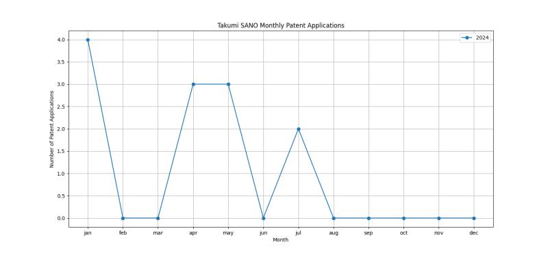
Patent Filing Activity
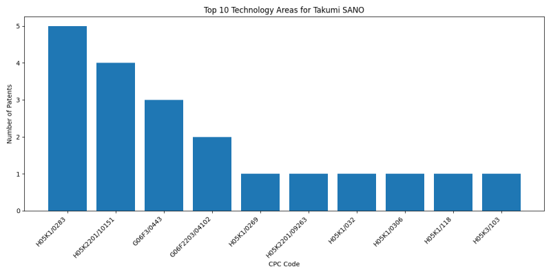
Technology Areas
List of Technology Areas
- H05K1/0283 (PRINTED CIRCUITS; CASINGS OR CONSTRUCTIONAL DETAILS OF ELECTRIC APPARATUS; MANUFACTURE OF ASSEMBLAGES OF ELECTRICAL COMPONENTS): 5 patents
- H05K2201/10151 (PRINTED CIRCUITS; CASINGS OR CONSTRUCTIONAL DETAILS OF ELECTRIC APPARATUS; MANUFACTURE OF ASSEMBLAGES OF ELECTRICAL COMPONENTS): 4 patents
- G06F3/0443 ({using a single layer of sensing electrodes}): 3 patents
- G06F2203/04102 (ELECTRIC DIGITAL DATA PROCESSING (computer systems based on specific computational models): 2 patents
- H05K1/0269 ({Spark gaps}): 1 patents
- H05K2201/09263 (PRINTED CIRCUITS; CASINGS OR CONSTRUCTIONAL DETAILS OF ELECTRIC APPARATUS; MANUFACTURE OF ASSEMBLAGES OF ELECTRICAL COMPONENTS): 1 patents
- H05K1/032 (Use of materials for the substrate): 1 patents
- H05K1/0306 (Use of materials for the substrate): 1 patents
- H05K1/118 (PRINTED CIRCUITS; CASINGS OR CONSTRUCTIONAL DETAILS OF ELECTRIC APPARATUS; MANUFACTURE OF ASSEMBLAGES OF ELECTRICAL COMPONENTS): 1 patents
- H05K3/103 (PRINTED CIRCUITS; CASINGS OR CONSTRUCTIONAL DETAILS OF ELECTRIC APPARATUS; MANUFACTURE OF ASSEMBLAGES OF ELECTRICAL COMPONENTS): 1 patents
- H05K2201/10106 (PRINTED CIRCUITS; CASINGS OR CONSTRUCTIONAL DETAILS OF ELECTRIC APPARATUS; MANUFACTURE OF ASSEMBLAGES OF ELECTRICAL COMPONENTS): 1 patents
- G06F3/04146 ({using pressure sensitive conductive elements delivering a boolean signal and located between crossing sensing lines, e.g. located between X and Y sensing line layers}): 1 patents
- G01L1/205 (MEASURING FORCE, STRESS, TORQUE, WORK, MECHANICAL POWER, MECHANICAL EFFICIENCY, OR FLUID PRESSURE (weighing): 1 patents
- G06F3/0412 ({Digitisers structurally integrated in a display}): 1 patents
- G06F2203/04105 (ELECTRIC DIGITAL DATA PROCESSING (computer systems based on specific computational models): 1 patents
- G06F3/044 (by capacitive means): 1 patents
- G06F2203/04108 (ELECTRIC DIGITAL DATA PROCESSING (computer systems based on specific computational models): 1 patents
- G06F3/04166 ({Details of scanning methods, e.g. sampling time, grouping of sub areas or time sharing with display driving (Synchronisation with the driving of the display or the backlighting unit to avoid interferences generated internally): 1 patents
- G06F3/0446 ({using a grid-like structure of electrodes in at least two directions, e.g. using row and column electrodes}): 1 patents
- H01L23/5386 (the interconnection structure between a plurality of semiconductor chips being formed on, or in, insulating substrates ({): 1 patents
- H01L23/5387 ({Flexible insulating substrates (): 1 patents
- H01L25/18 (the devices being of types provided for in two or more different subgroups of the same main group of groups): 1 patents
- H01L27/124 (the substrate being other than a semiconductor body, e.g. an insulating body): 1 patents
- H01L25/16 (the devices being of types provided for in two or more different main groups of groups): 1 patents
- H01L27/1218 (the substrate being other than a semiconductor body, e.g. an insulating body): 1 patents
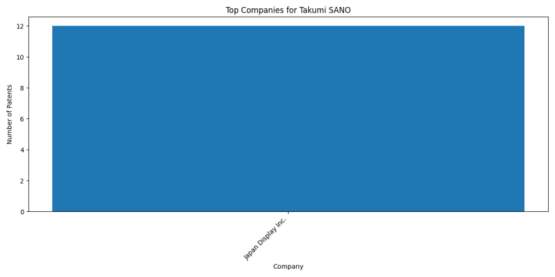
Companies
List of Companies
- Japan Display Inc.: 12 patents
Collaborators
- Masatomo HISHINUMA (6 collaborations)
- Yasushi TOMIOKA (2 collaborations)
- Akio MURAYAMA (2 collaborations)
- Shinichiro OKA (2 collaborations)
- Yosuke HYODO (1 collaborations)
- Hiroumi KINJO (1 collaborations)
Subcategories
This category has the following 4 subcategories, out of 4 total.


