Difference between revisions of "Category:Hajime WATAKABE"
Jump to navigation
Jump to search
Wikipatents (talk | contribs) (Updating Category:Hajime_WATAKABE) |
Wikipatents (talk | contribs) (Updating Category:Hajime_WATAKABE) |
||
| Line 2: | Line 2: | ||
=== Executive Summary === | === Executive Summary === | ||
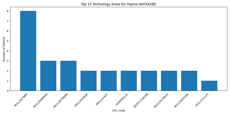
| − | Hajime WATAKABE is an inventor who has filed 13 patents. Their primary areas of innovation include | + | Hajime WATAKABE is an inventor who has filed 13 patents. Their primary areas of innovation include SEMICONDUCTOR DEVICES NOT COVERED BY CLASS (8 patents), {of devices having semiconductor bodies not comprising group 14 or group 13/15 materials (comprising selenium or tellurium in uncombined form other than as impurities in semiconductor bodies of other materials, comprising cuprous oxide or cuprous iodide (3 patents), SEMICONDUCTOR DEVICES NOT COVERED BY CLASS (3 patents), and they have worked with companies such as Japan Display Inc. (13 patents). Their most frequent collaborators include [[Category:Masashi TSUBUKU|Masashi TSUBUKU]] (10 collaborations), [[Category:Toshinari SASAKI|Toshinari SASAKI]] (10 collaborations), [[Category:Takaya TAMARU|Takaya TAMARU]] (9 collaborations). |
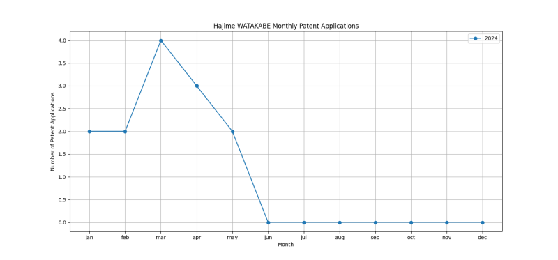
=== Patent Filing Activity === | === Patent Filing Activity === | ||
| Line 11: | Line 11: | ||
==== List of Technology Areas ==== | ==== List of Technology Areas ==== | ||
| − | * [[:Category:CPC_H01L29/7869|H01L29/7869]] ( | + | * [[:Category:CPC_H01L29/7869|H01L29/7869]] (SEMICONDUCTOR DEVICES NOT COVERED BY CLASS): 8 patents |
| − | * [[:Category:CPC_H01L29/66969|H01L29/66969]] ( | + | * [[:Category:CPC_H01L29/66969|H01L29/66969]] ({of devices having semiconductor bodies not comprising group 14 or group 13/15 materials (comprising selenium or tellurium in uncombined form other than as impurities in semiconductor bodies of other materials, comprising cuprous oxide or cuprous iodide): 3 patents |
| − | * [[:Category:CPC_H01L29/78696|H01L29/78696]] ( | + | * [[:Category:CPC_H01L29/78696|H01L29/78696]] (SEMICONDUCTOR DEVICES NOT COVERED BY CLASS): 3 patents |
| − | * [[:Category:CPC_H01L29/4908|H01L29/4908]] ( | + | * [[:Category:CPC_H01L29/4908|H01L29/4908]] (SEMICONDUCTOR DEVICES NOT COVERED BY CLASS): 2 patents |
| − | * [[:Category:CPC_H01L21/425|H01L21/425]] ( | + | * [[:Category:CPC_H01L21/425|H01L21/425]] (producing ion implantation): 2 patents |
| − | * [[:Category:CPC_H10K59/131|H10K59/131]] ( | + | * [[:Category:CPC_H10K59/131|H10K59/131]] (ORGANIC ELECTRIC SOLID-STATE DEVICES): 2 patents |
| − | * [[:Category:CPC_G02F1/136286|G02F1/136286]] ( | + | * [[:Category:CPC_G02F1/136286|G02F1/136286]] (based on liquid crystals, e.g. single liquid crystal display cells): 2 patents |
| − | * [[:Category:CPC_H01L29/78633|H01L29/78633]] ( | + | * [[:Category:CPC_H01L29/78633|H01L29/78633]] (SEMICONDUCTOR DEVICES NOT COVERED BY CLASS): 2 patents |
| − | * [[:Category:CPC_H01L29/42384|H01L29/42384]] ( | + | * [[:Category:CPC_H01L29/42384|H01L29/42384]] (SEMICONDUCTOR DEVICES NOT COVERED BY CLASS): 2 patents |
| − | * [[:Category:CPC_H01L27/1225|H01L27/1225]] ( | + | * [[:Category:CPC_H01L27/1225|H01L27/1225]] (the substrate being other than a semiconductor body, e.g. an insulating body): 1 patents |
| − | * [[:Category:CPC_H01L27/1285|H01L27/1285]] ( | + | * [[:Category:CPC_H01L27/1285|H01L27/1285]] (the substrate being other than a semiconductor body, e.g. an insulating body): 1 patents |
| − | * [[:Category:CPC_H01L29/66742|H01L29/66742]] ( | + | * [[:Category:CPC_H01L29/66742|H01L29/66742]] (SEMICONDUCTOR DEVICES NOT COVERED BY CLASS): 1 patents |
| − | * [[:Category:CPC_H01L21/02667|H01L21/02667]] ( | + | * [[:Category:CPC_H01L21/02667|H01L21/02667]] (SEMICONDUCTOR DEVICES NOT COVERED BY CLASS): 1 patents |
| − | * [[:Category:CPC_H01L29/04|H01L29/04]] ( | + | * [[:Category:CPC_H01L29/04|H01L29/04]] (SEMICONDUCTOR DEVICES NOT COVERED BY CLASS): 1 patents |
| − | * [[:Category:CPC_H01L21/02595|H01L21/02595]] ( | + | * [[:Category:CPC_H01L21/02595|H01L21/02595]] (SEMICONDUCTOR DEVICES NOT COVERED BY CLASS): 1 patents |
| − | * [[:Category:CPC_H01L21/02609|H01L21/02609]] ( | + | * [[:Category:CPC_H01L21/02609|H01L21/02609]] (SEMICONDUCTOR DEVICES NOT COVERED BY CLASS): 1 patents |
| − | * [[:Category:CPC_H01L21/02554|H01L21/02554]] ( | + | * [[:Category:CPC_H01L21/02554|H01L21/02554]] (SEMICONDUCTOR DEVICES NOT COVERED BY CLASS): 1 patents |
| − | * [[:Category:CPC_H01L21/02129|H01L21/02129]] ( | + | * [[:Category:CPC_H01L21/02129|H01L21/02129]] ({the material being boron or phosphorus doped silicon oxides, e.g. BPSG, BSG or PSG}): 1 patents |
| − | * [[:Category:CPC_H01L29/401|H01L29/401]] ( | + | * [[:Category:CPC_H01L29/401|H01L29/401]] (SEMICONDUCTOR DEVICES NOT COVERED BY CLASS): 1 patents |
| − | * [[:Category:CPC_H10K59/1213|H10K59/1213]] ( | + | * [[:Category:CPC_H10K59/1213|H10K59/1213]] (ORGANIC ELECTRIC SOLID-STATE DEVICES): 1 patents |
| − | * [[:Category:CPC_G02F1/136227|G02F1/136227]] ( | + | * [[:Category:CPC_G02F1/136227|G02F1/136227]] (based on liquid crystals, e.g. single liquid crystal display cells): 1 patents |
| − | * [[:Category:CPC_G02F1/13685|G02F1/13685]] ( | + | * [[:Category:CPC_G02F1/13685|G02F1/13685]] (based on liquid crystals, e.g. single liquid crystal display cells): 1 patents |
| − | * [[:Category:CPC_G06F3/044|G06F3/044]] ( | + | * [[:Category:CPC_G06F3/044|G06F3/044]] (by capacitive means): 1 patents |
| − | * [[:Category:CPC_H01L29/0603|H01L29/0603]] ( | + | * [[:Category:CPC_H01L29/0603|H01L29/0603]] (SEMICONDUCTOR DEVICES NOT COVERED BY CLASS): 1 patents |
| − | * [[:Category:CPC_G02F1/1368|G02F1/1368]] ( | + | * [[:Category:CPC_G02F1/1368|G02F1/1368]] (based on liquid crystals, e.g. single liquid crystal display cells): 1 patents |
| − | * [[:Category:CPC_G02F1/136209|G02F1/136209]] ( | + | * [[:Category:CPC_G02F1/136209|G02F1/136209]] (based on liquid crystals, e.g. single liquid crystal display cells): 1 patents |
| − | * [[:Category:CPC_G02F1/136277|G02F1/136277]] ( | + | * [[:Category:CPC_G02F1/136277|G02F1/136277]] (based on liquid crystals, e.g. single liquid crystal display cells): 1 patents |
| − | * [[:Category:CPC_H01L29/78672|H01L29/78672]] ( | + | * [[:Category:CPC_H01L29/78672|H01L29/78672]] (SEMICONDUCTOR DEVICES NOT COVERED BY CLASS): 1 patents |
| − | * [[:Category:CPC_H10K50/865|H10K50/865]] ( | + | * [[:Category:CPC_H10K50/865|H10K50/865]] (ORGANIC ELECTRIC SOLID-STATE DEVICES): 1 patents |
| − | * [[:Category:CPC_H01L21/02565|H01L21/02565]] ( | + | * [[:Category:CPC_H01L21/02565|H01L21/02565]] (SEMICONDUCTOR DEVICES NOT COVERED BY CLASS): 1 patents |
| − | * [[:Category:CPC_H01L21/02631|H01L21/02631]] ( | + | * [[:Category:CPC_H01L21/02631|H01L21/02631]] (SEMICONDUCTOR DEVICES NOT COVERED BY CLASS): 1 patents |
| − | * [[:Category:CPC_H01L21/47576|H01L21/47576]] ( | + | * [[:Category:CPC_H01L21/47576|H01L21/47576]] (Organic layers, e.g. photoresist (): 1 patents |
| − | * [[:Category:CPC_H01L2029/42388|H01L2029/42388]] ( | + | * [[:Category:CPC_H01L2029/42388|H01L2029/42388]] (SEMICONDUCTOR DEVICES NOT COVERED BY CLASS): 1 patents |
| − | * [[:Category:CPC_H01L27/14643|H01L27/14643]] ( | + | * [[:Category:CPC_H01L27/14643|H01L27/14643]] ({Photodiode arrays; MOS imagers}): 1 patents |
| − | * [[:Category:CPC_H01L27/1461|H01L27/1461]] ( | + | * [[:Category:CPC_H01L27/1461|H01L27/1461]] ({characterised by the photosensitive area}): 1 patents |
| − | * [[:Category:CPC_H01L27/14636|H01L27/14636]] ( | + | * [[:Category:CPC_H01L27/14636|H01L27/14636]] ({Interconnect structures}): 1 patents |
| − | * [[:Category:CPC_H01L27/14689|H01L27/14689]] ( | + | * [[:Category:CPC_H01L27/14689|H01L27/14689]] ({MOS based technologies}): 1 patents |
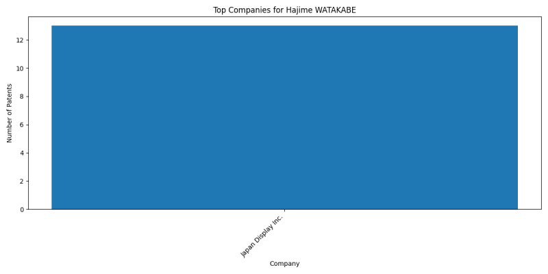
=== Companies === | === Companies === | ||
Latest revision as of 12:54, 18 July 2024
Contents
Hajime WATAKABE
Executive Summary
Hajime WATAKABE is an inventor who has filed 13 patents. Their primary areas of innovation include SEMICONDUCTOR DEVICES NOT COVERED BY CLASS (8 patents), {of devices having semiconductor bodies not comprising group 14 or group 13/15 materials (comprising selenium or tellurium in uncombined form other than as impurities in semiconductor bodies of other materials, comprising cuprous oxide or cuprous iodide (3 patents), SEMICONDUCTOR DEVICES NOT COVERED BY CLASS (3 patents), and they have worked with companies such as Japan Display Inc. (13 patents). Their most frequent collaborators include (10 collaborations), (10 collaborations), (9 collaborations).
Patent Filing Activity
Technology Areas
List of Technology Areas
- H01L29/7869 (SEMICONDUCTOR DEVICES NOT COVERED BY CLASS): 8 patents
- H01L29/66969 ({of devices having semiconductor bodies not comprising group 14 or group 13/15 materials (comprising selenium or tellurium in uncombined form other than as impurities in semiconductor bodies of other materials, comprising cuprous oxide or cuprous iodide): 3 patents
- H01L29/78696 (SEMICONDUCTOR DEVICES NOT COVERED BY CLASS): 3 patents
- H01L29/4908 (SEMICONDUCTOR DEVICES NOT COVERED BY CLASS): 2 patents
- H01L21/425 (producing ion implantation): 2 patents
- H10K59/131 (ORGANIC ELECTRIC SOLID-STATE DEVICES): 2 patents
- G02F1/136286 (based on liquid crystals, e.g. single liquid crystal display cells): 2 patents
- H01L29/78633 (SEMICONDUCTOR DEVICES NOT COVERED BY CLASS): 2 patents
- H01L29/42384 (SEMICONDUCTOR DEVICES NOT COVERED BY CLASS): 2 patents
- H01L27/1225 (the substrate being other than a semiconductor body, e.g. an insulating body): 1 patents
- H01L27/1285 (the substrate being other than a semiconductor body, e.g. an insulating body): 1 patents
- H01L29/66742 (SEMICONDUCTOR DEVICES NOT COVERED BY CLASS): 1 patents
- H01L21/02667 (SEMICONDUCTOR DEVICES NOT COVERED BY CLASS): 1 patents
- H01L29/04 (SEMICONDUCTOR DEVICES NOT COVERED BY CLASS): 1 patents
- H01L21/02595 (SEMICONDUCTOR DEVICES NOT COVERED BY CLASS): 1 patents
- H01L21/02609 (SEMICONDUCTOR DEVICES NOT COVERED BY CLASS): 1 patents
- H01L21/02554 (SEMICONDUCTOR DEVICES NOT COVERED BY CLASS): 1 patents
- H01L21/02129 ({the material being boron or phosphorus doped silicon oxides, e.g. BPSG, BSG or PSG}): 1 patents
- H01L29/401 (SEMICONDUCTOR DEVICES NOT COVERED BY CLASS): 1 patents
- H10K59/1213 (ORGANIC ELECTRIC SOLID-STATE DEVICES): 1 patents
- G02F1/136227 (based on liquid crystals, e.g. single liquid crystal display cells): 1 patents
- G02F1/13685 (based on liquid crystals, e.g. single liquid crystal display cells): 1 patents
- G06F3/044 (by capacitive means): 1 patents
- H01L29/0603 (SEMICONDUCTOR DEVICES NOT COVERED BY CLASS): 1 patents
- G02F1/1368 (based on liquid crystals, e.g. single liquid crystal display cells): 1 patents
- G02F1/136209 (based on liquid crystals, e.g. single liquid crystal display cells): 1 patents
- G02F1/136277 (based on liquid crystals, e.g. single liquid crystal display cells): 1 patents
- H01L29/78672 (SEMICONDUCTOR DEVICES NOT COVERED BY CLASS): 1 patents
- H10K50/865 (ORGANIC ELECTRIC SOLID-STATE DEVICES): 1 patents
- H01L21/02565 (SEMICONDUCTOR DEVICES NOT COVERED BY CLASS): 1 patents
- H01L21/02631 (SEMICONDUCTOR DEVICES NOT COVERED BY CLASS): 1 patents
- H01L21/47576 (Organic layers, e.g. photoresist (): 1 patents
- H01L2029/42388 (SEMICONDUCTOR DEVICES NOT COVERED BY CLASS): 1 patents
- H01L27/14643 ({Photodiode arrays; MOS imagers}): 1 patents
- H01L27/1461 ({characterised by the photosensitive area}): 1 patents
- H01L27/14636 ({Interconnect structures}): 1 patents
- H01L27/14689 ({MOS based technologies}): 1 patents
Companies
List of Companies
- Japan Display Inc.: 13 patents
Collaborators
- Masashi TSUBUKU (10 collaborations)
- Toshinari SASAKI (10 collaborations)
- Takaya TAMARU (9 collaborations)
- Akihiro HANADA (5 collaborations)
- Ryo ONODERA (4 collaborations)
- Toshihide JINNAI (2 collaborations)
- Marina MOCHIZUKI (2 collaborations)
- Isao SUZUMURA (2 collaborations)
- Takay TAMARU (1 collaborations)
- Fumiya KIMURA (1 collaborations)
Subcategories
This category has the following 5 subcategories, out of 5 total.


