Difference between revisions of "Category:Takayuki OHBA"
Jump to navigation
Jump to search
Wikipatents (talk | contribs) (Updating Category:Takayuki_OHBA) |
Wikipatents (talk | contribs) (Updating Category:Takayuki_OHBA) |
||
| Line 2: | Line 2: | ||
=== Executive Summary === | === Executive Summary === | ||
| − | Takayuki OHBA is an inventor who has filed 5 patents. Their primary areas of innovation include | + | Takayuki OHBA is an inventor who has filed 5 patents. Their primary areas of innovation include {Geometry or} layout of the interconnection structure {( (2 patents), to produce devices, e.g. integrated circuits, each consisting of a plurality of components (2 patents), SEMICONDUCTOR DEVICES NOT COVERED BY CLASS (2 patents), and they have worked with companies such as ADVANTEST CORPORATION (5 patents). Their most frequent collaborators include [[Category:Shinji SUGATANI|Shinji SUGATANI]] (5 collaborations), [[Category:Koji SAKUI|Koji SAKUI]] (4 collaborations), [[Category:Norio CHUJO|Norio CHUJO]] (4 collaborations). |
=== Patent Filing Activity === | === Patent Filing Activity === | ||
| Line 11: | Line 11: | ||
==== List of Technology Areas ==== | ==== List of Technology Areas ==== | ||
| − | * [[:Category:CPC_H01L23/528|H01L23/528]] ( | + | * [[:Category:CPC_H01L23/528|H01L23/528]] ({Geometry or} layout of the interconnection structure {(): 2 patents |
| − | * [[:Category:CPC_H01L21/823871|H01L21/823871]] ( | + | * [[:Category:CPC_H01L21/823871|H01L21/823871]] (to produce devices, e.g. integrated circuits, each consisting of a plurality of components): 2 patents |
| − | * [[:Category:CPC_H01L27/092|H01L27/092]] ( | + | * [[:Category:CPC_H01L27/092|H01L27/092]] (SEMICONDUCTOR DEVICES NOT COVERED BY CLASS): 2 patents |
| − | * [[:Category:CPC_H01L29/0673|H01L29/0673]] ( | + | * [[:Category:CPC_H01L29/0673|H01L29/0673]] (SEMICONDUCTOR DEVICES NOT COVERED BY CLASS): 2 patents |
| − | * [[:Category:CPC_H01L29/42392|H01L29/42392]] ( | + | * [[:Category:CPC_H01L29/42392|H01L29/42392]] (SEMICONDUCTOR DEVICES NOT COVERED BY CLASS): 2 patents |
| − | * [[:Category:CPC_H01L29/775|H01L29/775]] ( | + | * [[:Category:CPC_H01L29/775|H01L29/775]] (SEMICONDUCTOR DEVICES NOT COVERED BY CLASS): 2 patents |
| − | * [[:Category:CPC_H01L24/08|H01L24/08]] ( | + | * [[:Category:CPC_H01L24/08|H01L24/08]] (SEMICONDUCTOR DEVICES NOT COVERED BY CLASS): 2 patents |
| − | * [[:Category:CPC_H01L21/76898|H01L21/76898]] ( | + | * [[:Category:CPC_H01L21/76898|H01L21/76898]] ({formed through a semiconductor substrate}): 2 patents |
| − | * [[:Category:CPC_H01L23/481|H01L23/481]] ( | + | * [[:Category:CPC_H01L23/481|H01L23/481]] (Arrangements for conducting electric current to or from the solid state body in operation, e.g. leads, terminal arrangements {; Selection of materials therefor}): 2 patents |
| − | * [[:Category:CPC_H01L23/5226|H01L23/5226]] ( | + | * [[:Category:CPC_H01L23/5226|H01L23/5226]] (SEMICONDUCTOR DEVICES NOT COVERED BY CLASS): 2 patents |
| − | * [[:Category:CPC_H01L24/80|H01L24/80]] ( | + | * [[:Category:CPC_H01L24/80|H01L24/80]] ({Methods for connecting semiconductor or other solid state bodies using means for bonding being attached to, or being formed on, the surface to be connected}): 2 patents |
| − | * [[:Category:CPC_H01L2224/08145|H01L2224/08145]] ( | + | * [[:Category:CPC_H01L2224/08145|H01L2224/08145]] (SEMICONDUCTOR DEVICES NOT COVERED BY CLASS): 2 patents |
| − | * [[:Category:CPC_H01L2224/80895|H01L2224/80895]] ( | + | * [[:Category:CPC_H01L2224/80895|H01L2224/80895]] (SEMICONDUCTOR DEVICES NOT COVERED BY CLASS): 2 patents |
| − | * [[:Category:CPC_H01L2224/80896|H01L2224/80896]] ( | + | * [[:Category:CPC_H01L2224/80896|H01L2224/80896]] (SEMICONDUCTOR DEVICES NOT COVERED BY CLASS): 2 patents |
| − | * [[:Category:CPC_H01L23/367|H01L23/367]] ( | + | * [[:Category:CPC_H01L23/367|H01L23/367]] (Cooling facilitated by shape of device {(): 1 patents |
| − | * [[:Category:CPC_H01L21/56|H01L21/56]] ( | + | * [[:Category:CPC_H01L21/56|H01L21/56]] (SEMICONDUCTOR DEVICES NOT COVERED BY CLASS): 1 patents |
| − | * [[:Category:CPC_H01L23/291|H01L23/291]] ( | + | * [[:Category:CPC_H01L23/291|H01L23/291]] (SEMICONDUCTOR DEVICES NOT COVERED BY CLASS): 1 patents |
| − | * [[:Category:CPC_H01L23/3128|H01L23/3128]] ( | + | * [[:Category:CPC_H01L23/3128|H01L23/3128]] (SEMICONDUCTOR DEVICES NOT COVERED BY CLASS): 1 patents |
| − | * [[:Category:CPC_H01L23/3135|H01L23/3135]] ( | + | * [[:Category:CPC_H01L23/3135|H01L23/3135]] (SEMICONDUCTOR DEVICES NOT COVERED BY CLASS): 1 patents |
| − | * [[:Category:CPC_H01L23/427|H01L23/427]] ( | + | * [[:Category:CPC_H01L23/427|H01L23/427]] (Cooling by change of state, e.g. use of heat pipes {(by liquefied gas): 1 patents |
| − | * [[:Category:CPC_H01L23/544|H01L23/544]] ( | + | * [[:Category:CPC_H01L23/544|H01L23/544]] (Marks applied to semiconductor devices {or parts}, e.g. registration marks, {alignment structures, wafer maps (test patterns for characterising or monitoring manufacturing processes): 1 patents |
| − | * [[:Category:CPC_H01L25/0655|H01L25/0655]] ( | + | * [[:Category:CPC_H01L25/0655|H01L25/0655]] (SEMICONDUCTOR DEVICES NOT COVERED BY CLASS): 1 patents |
| − | * [[:Category:CPC_H01L25/50|H01L25/50]] ( | + | * [[:Category:CPC_H01L25/50|H01L25/50]] ({Multistep manufacturing processes of assemblies consisting of devices, each device being of a type provided for in group): 1 patents |
| − | * [[:Category:CPC_H01L24/13|H01L24/13]] ( | + | * [[:Category:CPC_H01L24/13|H01L24/13]] (SEMICONDUCTOR DEVICES NOT COVERED BY CLASS): 1 patents |
=== Companies === | === Companies === | ||
Latest revision as of 15:54, 21 July 2024
Contents
Takayuki OHBA
Executive Summary
Takayuki OHBA is an inventor who has filed 5 patents. Their primary areas of innovation include {Geometry or} layout of the interconnection structure {( (2 patents), to produce devices, e.g. integrated circuits, each consisting of a plurality of components (2 patents), SEMICONDUCTOR DEVICES NOT COVERED BY CLASS (2 patents), and they have worked with companies such as ADVANTEST CORPORATION (5 patents). Their most frequent collaborators include (5 collaborations), (4 collaborations), (4 collaborations).
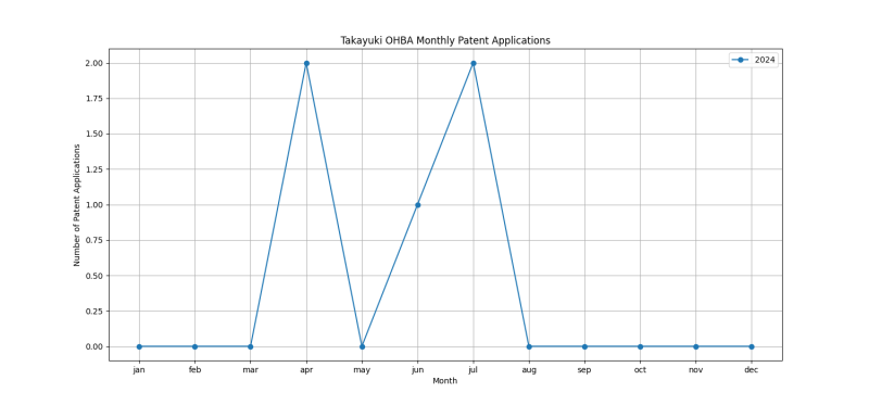
Patent Filing Activity
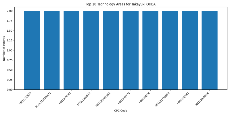
Technology Areas
List of Technology Areas
- H01L23/528 ({Geometry or} layout of the interconnection structure {(): 2 patents
- H01L21/823871 (to produce devices, e.g. integrated circuits, each consisting of a plurality of components): 2 patents
- H01L27/092 (SEMICONDUCTOR DEVICES NOT COVERED BY CLASS): 2 patents
- H01L29/0673 (SEMICONDUCTOR DEVICES NOT COVERED BY CLASS): 2 patents
- H01L29/42392 (SEMICONDUCTOR DEVICES NOT COVERED BY CLASS): 2 patents
- H01L29/775 (SEMICONDUCTOR DEVICES NOT COVERED BY CLASS): 2 patents
- H01L24/08 (SEMICONDUCTOR DEVICES NOT COVERED BY CLASS): 2 patents
- H01L21/76898 ({formed through a semiconductor substrate}): 2 patents
- H01L23/481 (Arrangements for conducting electric current to or from the solid state body in operation, e.g. leads, terminal arrangements {; Selection of materials therefor}): 2 patents
- H01L23/5226 (SEMICONDUCTOR DEVICES NOT COVERED BY CLASS): 2 patents
- H01L24/80 ({Methods for connecting semiconductor or other solid state bodies using means for bonding being attached to, or being formed on, the surface to be connected}): 2 patents
- H01L2224/08145 (SEMICONDUCTOR DEVICES NOT COVERED BY CLASS): 2 patents
- H01L2224/80895 (SEMICONDUCTOR DEVICES NOT COVERED BY CLASS): 2 patents
- H01L2224/80896 (SEMICONDUCTOR DEVICES NOT COVERED BY CLASS): 2 patents
- H01L23/367 (Cooling facilitated by shape of device {(): 1 patents
- H01L21/56 (SEMICONDUCTOR DEVICES NOT COVERED BY CLASS): 1 patents
- H01L23/291 (SEMICONDUCTOR DEVICES NOT COVERED BY CLASS): 1 patents
- H01L23/3128 (SEMICONDUCTOR DEVICES NOT COVERED BY CLASS): 1 patents
- H01L23/3135 (SEMICONDUCTOR DEVICES NOT COVERED BY CLASS): 1 patents
- H01L23/427 (Cooling by change of state, e.g. use of heat pipes {(by liquefied gas): 1 patents
- H01L23/544 (Marks applied to semiconductor devices {or parts}, e.g. registration marks, {alignment structures, wafer maps (test patterns for characterising or monitoring manufacturing processes): 1 patents
- H01L25/0655 (SEMICONDUCTOR DEVICES NOT COVERED BY CLASS): 1 patents
- H01L25/50 ({Multistep manufacturing processes of assemblies consisting of devices, each device being of a type provided for in group): 1 patents
- H01L24/13 (SEMICONDUCTOR DEVICES NOT COVERED BY CLASS): 1 patents
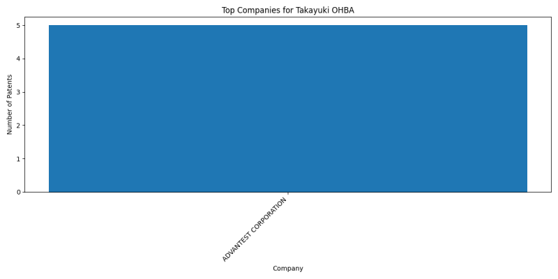
Companies
List of Companies
- ADVANTEST CORPORATION: 5 patents
Collaborators
- Shinji SUGATANI (5 collaborations)
- Koji SAKUI (4 collaborations)
- Norio CHUJO (4 collaborations)
- Tadashi FUKUDA (2 collaborations)
Subcategories
This category has the following 5 subcategories, out of 5 total.


