Difference between revisions of "Category:Yoshikatsu IMAZEKI"
Wikipatents (talk | contribs) (Updating Category:Yoshikatsu_IMAZEKI) |
Wikipatents (talk | contribs) (Updating Category:Yoshikatsu_IMAZEKI) |
||
| Line 2: | Line 2: | ||
=== Executive Summary === | === Executive Summary === | ||
| − | Yoshikatsu IMAZEKI is an inventor who has filed 10 patents. Their primary areas of innovation include | + | Yoshikatsu IMAZEKI is an inventor who has filed 10 patents. Their primary areas of innovation include {Colour filters} (5 patents), OPTICAL DEVICES OR ARRANGEMENTS FOR THE CONTROL OF LIGHT BY MODIFICATION OF THE OPTICAL PROPERTIES OF THE MEDIA OF THE ELEMENTS INVOLVED THEREIN; NON-LINEAR OPTICS; FREQUENCY-CHANGING OF LIGHT; OPTICAL LOGIC ELEMENTS; OPTICAL ANALOGUE/DIGITAL CONVERTERS (5 patents), LAYERED PRODUCTS, i.e. PRODUCTS BUILT-UP OF STRATA OF FLAT OR NON-FLAT, e.g. CELLULAR OR HONEYCOMB, FORM (4 patents), and they have worked with companies such as Japan Display Inc. (10 patents). Their most frequent collaborators include [[Category:Shuichi OSAWA|Shuichi OSAWA]] (9 collaborations), [[Category:Yoichi KAMIJO|Yoichi KAMIJO]] (9 collaborations), [[Category:Koichi MIYASAKA|Koichi MIYASAKA]] (9 collaborations). |
=== Patent Filing Activity === | === Patent Filing Activity === | ||
| Line 11: | Line 11: | ||
==== List of Technology Areas ==== | ==== List of Technology Areas ==== | ||
| − | * [[:Category:CPC_G02F1/133514|G02F1/133514]] ( | + | * [[:Category:CPC_G02F1/133514|G02F1/133514]] ({Colour filters}): 5 patents |
| − | * [[:Category:CPC_G02F2202/28|G02F2202/28]] ( | + | * [[:Category:CPC_G02F2202/28|G02F2202/28]] (OPTICAL DEVICES OR ARRANGEMENTS FOR THE CONTROL OF LIGHT BY MODIFICATION OF THE OPTICAL PROPERTIES OF THE MEDIA OF THE ELEMENTS INVOLVED THEREIN; NON-LINEAR OPTICS; FREQUENCY-CHANGING OF LIGHT; OPTICAL LOGIC ELEMENTS; OPTICAL ANALOGUE/DIGITAL CONVERTERS): 5 patents |
| − | * [[:Category:CPC_B32B37/12|B32B37/12]] ( | + | * [[:Category:CPC_B32B37/12|B32B37/12]] (LAYERED PRODUCTS, i.e. PRODUCTS BUILT-UP OF STRATA OF FLAT OR NON-FLAT, e.g. CELLULAR OR HONEYCOMB, FORM): 4 patents |
| − | * [[:Category:CPC_B32B2457/20|B32B2457/20]] ( | + | * [[:Category:CPC_B32B2457/20|B32B2457/20]] (LAYERED PRODUCTS, i.e. PRODUCTS BUILT-UP OF STRATA OF FLAT OR NON-FLAT, e.g. CELLULAR OR HONEYCOMB, FORM): 2 patents |
| − | * [[:Category:CPC_B32B7/12|B32B7/12]] ( | + | * [[:Category:CPC_B32B7/12|B32B7/12]] (using interposed adhesives or interposed materials with bonding properties): 2 patents |
| − | * [[:Category:CPC_B32B37/10|B32B37/10]] ( | + | * [[:Category:CPC_B32B37/10|B32B37/10]] (LAYERED PRODUCTS, i.e. PRODUCTS BUILT-UP OF STRATA OF FLAT OR NON-FLAT, e.g. CELLULAR OR HONEYCOMB, FORM): 2 patents |
| − | * [[:Category:CPC_B32B2037/1253|B32B2037/1253]] ( | + | * [[:Category:CPC_B32B2037/1253|B32B2037/1253]] (LAYERED PRODUCTS, i.e. PRODUCTS BUILT-UP OF STRATA OF FLAT OR NON-FLAT, e.g. CELLULAR OR HONEYCOMB, FORM): 2 patents |
| − | * [[:Category:CPC_B32B2457/202|B32B2457/202]] ( | + | * [[:Category:CPC_B32B2457/202|B32B2457/202]] (LAYERED PRODUCTS, i.e. PRODUCTS BUILT-UP OF STRATA OF FLAT OR NON-FLAT, e.g. CELLULAR OR HONEYCOMB, FORM): 2 patents |
| − | * [[:Category:CPC_G02F1/133637|G02F1/133637]] ( | + | * [[:Category:CPC_G02F1/133637|G02F1/133637]] ({Illuminating devices}): 2 patents |
| − | * [[:Category:CPC_G06F3/0446|G06F3/0446]] ( | + | * [[:Category:CPC_G06F3/0446|G06F3/0446]] ({using a grid-like structure of electrodes in at least two directions, e.g. using row and column electrodes}): 1 patents |
| − | * [[:Category:CPC_G02F1/13338|G02F1/13338]] ( | + | * [[:Category:CPC_G02F1/13338|G02F1/13338]] ({Input devices, e.g. touch panels}): 1 patents |
| − | * [[:Category:CPC_G02F1/134309|G02F1/134309]] ( | + | * [[:Category:CPC_G02F1/134309|G02F1/134309]] ({characterised by their geometrical arrangement}): 1 patents |
| − | * [[:Category:CPC_G06V40/1306|G06V40/1306]] ( | + | * [[:Category:CPC_G06V40/1306|G06V40/1306]] (IMAGE OR VIDEO RECOGNITION OR UNDERSTANDING): 1 patents |
| − | * [[:Category:CPC_G02F1/1347|G02F1/1347]] ( | + | * [[:Category:CPC_G02F1/1347|G02F1/1347]] (Arrangement of liquid crystal layers or cells in which the final condition of one light beam is achieved by the addition of the effects of two or more layers or cells): 1 patents |
| − | * [[:Category:CPC_G02F1/133308|G02F1/133308]] ( | + | * [[:Category:CPC_G02F1/133308|G02F1/133308]] (Constructional arrangements; Operation of liquid crystal cells; Circuit arrangements (arrangements or circuits for control of liquid crystal elements in a matrix, not structurally associated with these elements): 1 patents |
| − | * [[:Category:CPC_G02F1/1339|G02F1/1339]] ( | + | * [[:Category:CPC_G02F1/1339|G02F1/1339]] (Constructional arrangements; Operation of liquid crystal cells; Circuit arrangements (arrangements or circuits for control of liquid crystal elements in a matrix, not structurally associated with these elements): 1 patents |
| − | * [[:Category:CPC_G02F1/133334|G02F1/133334]] ( | + | * [[:Category:CPC_G02F1/133334|G02F1/133334]] (Constructional arrangements; Operation of liquid crystal cells; Circuit arrangements (arrangements or circuits for control of liquid crystal elements in a matrix, not structurally associated with these elements): 1 patents |
| − | * [[:Category:CPC_G02F1/13452|G02F1/13452]] ( | + | * [[:Category:CPC_G02F1/13452|G02F1/13452]] ({Conductors connecting driver circuitry and terminals of panels}): 1 patents |
| − | * [[:Category:CPC_G02F1/13458|G02F1/13458]] ( | + | * [[:Category:CPC_G02F1/13458|G02F1/13458]] (Conductors connecting electrodes to cell terminals): 1 patents |
=== Companies === | === Companies === | ||
Latest revision as of 12:55, 18 July 2024
Contents
Yoshikatsu IMAZEKI
Executive Summary
Yoshikatsu IMAZEKI is an inventor who has filed 10 patents. Their primary areas of innovation include {Colour filters} (5 patents), OPTICAL DEVICES OR ARRANGEMENTS FOR THE CONTROL OF LIGHT BY MODIFICATION OF THE OPTICAL PROPERTIES OF THE MEDIA OF THE ELEMENTS INVOLVED THEREIN; NON-LINEAR OPTICS; FREQUENCY-CHANGING OF LIGHT; OPTICAL LOGIC ELEMENTS; OPTICAL ANALOGUE/DIGITAL CONVERTERS (5 patents), LAYERED PRODUCTS, i.e. PRODUCTS BUILT-UP OF STRATA OF FLAT OR NON-FLAT, e.g. CELLULAR OR HONEYCOMB, FORM (4 patents), and they have worked with companies such as Japan Display Inc. (10 patents). Their most frequent collaborators include (9 collaborations), (9 collaborations), (9 collaborations).
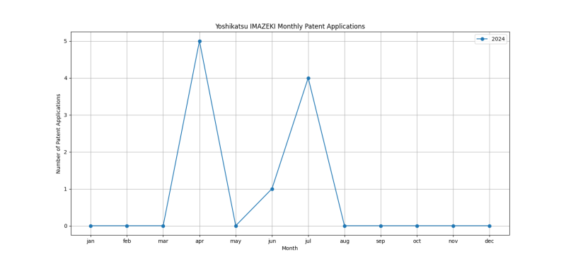
Patent Filing Activity
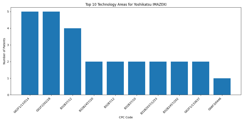
Technology Areas
List of Technology Areas
- G02F1/133514 ({Colour filters}): 5 patents
- G02F2202/28 (OPTICAL DEVICES OR ARRANGEMENTS FOR THE CONTROL OF LIGHT BY MODIFICATION OF THE OPTICAL PROPERTIES OF THE MEDIA OF THE ELEMENTS INVOLVED THEREIN; NON-LINEAR OPTICS; FREQUENCY-CHANGING OF LIGHT; OPTICAL LOGIC ELEMENTS; OPTICAL ANALOGUE/DIGITAL CONVERTERS): 5 patents
- B32B37/12 (LAYERED PRODUCTS, i.e. PRODUCTS BUILT-UP OF STRATA OF FLAT OR NON-FLAT, e.g. CELLULAR OR HONEYCOMB, FORM): 4 patents
- B32B2457/20 (LAYERED PRODUCTS, i.e. PRODUCTS BUILT-UP OF STRATA OF FLAT OR NON-FLAT, e.g. CELLULAR OR HONEYCOMB, FORM): 2 patents
- B32B7/12 (using interposed adhesives or interposed materials with bonding properties): 2 patents
- B32B37/10 (LAYERED PRODUCTS, i.e. PRODUCTS BUILT-UP OF STRATA OF FLAT OR NON-FLAT, e.g. CELLULAR OR HONEYCOMB, FORM): 2 patents
- B32B2037/1253 (LAYERED PRODUCTS, i.e. PRODUCTS BUILT-UP OF STRATA OF FLAT OR NON-FLAT, e.g. CELLULAR OR HONEYCOMB, FORM): 2 patents
- B32B2457/202 (LAYERED PRODUCTS, i.e. PRODUCTS BUILT-UP OF STRATA OF FLAT OR NON-FLAT, e.g. CELLULAR OR HONEYCOMB, FORM): 2 patents
- G02F1/133637 ({Illuminating devices}): 2 patents
- G06F3/0446 ({using a grid-like structure of electrodes in at least two directions, e.g. using row and column electrodes}): 1 patents
- G02F1/13338 ({Input devices, e.g. touch panels}): 1 patents
- G02F1/134309 ({characterised by their geometrical arrangement}): 1 patents
- G06V40/1306 (IMAGE OR VIDEO RECOGNITION OR UNDERSTANDING): 1 patents
- G02F1/1347 (Arrangement of liquid crystal layers or cells in which the final condition of one light beam is achieved by the addition of the effects of two or more layers or cells): 1 patents
- G02F1/133308 (Constructional arrangements; Operation of liquid crystal cells; Circuit arrangements (arrangements or circuits for control of liquid crystal elements in a matrix, not structurally associated with these elements): 1 patents
- G02F1/1339 (Constructional arrangements; Operation of liquid crystal cells; Circuit arrangements (arrangements or circuits for control of liquid crystal elements in a matrix, not structurally associated with these elements): 1 patents
- G02F1/133334 (Constructional arrangements; Operation of liquid crystal cells; Circuit arrangements (arrangements or circuits for control of liquid crystal elements in a matrix, not structurally associated with these elements): 1 patents
- G02F1/13452 ({Conductors connecting driver circuitry and terminals of panels}): 1 patents
- G02F1/13458 (Conductors connecting electrodes to cell terminals): 1 patents
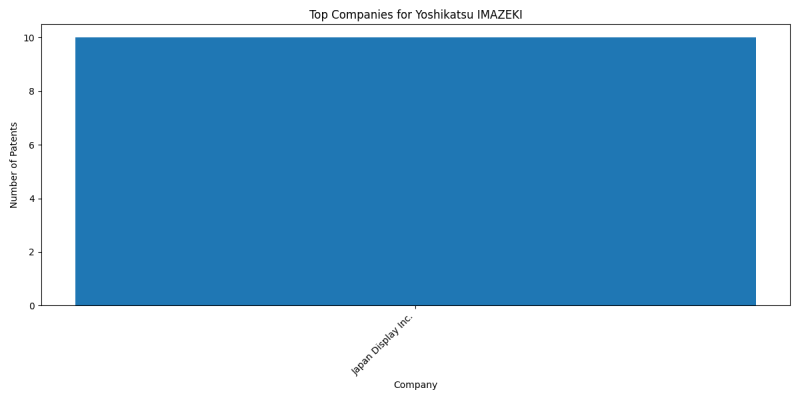
Companies
List of Companies
- Japan Display Inc.: 10 patents
Collaborators
- Shuichi OSAWA (9 collaborations)
- Yoichi KAMIJO (9 collaborations)
- Koichi MIYASAKA (9 collaborations)
- Yoshifumi KAMEI (9 collaborations)
- Toshinori UEHARA (1 collaborations)
- Takeo KOITO (1 collaborations)
- Kojiro IKEDA (1 collaborations)
Subcategories
This category has the following 7 subcategories, out of 7 total.


