Difference between revisions of "Category:Laura Wills Mirkarimi of Sunol CA (US)"
Jump to navigation
Jump to search
Wikipatents (talk | contribs) (Updating Category:Laura_Wills_Mirkarimi_of_Sunol_CA_(US)) |
Wikipatents (talk | contribs) (Updating Category:Laura_Wills_Mirkarimi_of_Sunol_CA_(US)) |
||
| Line 2: | Line 2: | ||
=== Executive Summary === | === Executive Summary === | ||
| − | Laura Wills Mirkarimi of Sunol CA (US) is an inventor who has filed | + | Laura Wills Mirkarimi of Sunol CA (US) is an inventor who has filed 7 patents. Their primary areas of innovation include SEMICONDUCTOR DEVICES NOT COVERED BY CLASS (4 patents), {Methods for connecting semiconductor or other solid state bodies using means for bonding being attached to, or being formed on, the surface to be connected} (4 patents), SEMICONDUCTOR DEVICES NOT COVERED BY CLASS (4 patents), and they have worked with companies such as ADEIA SEMICONDUCTOR BONDING TECHNOLOGIES INC. (7 patents). Their most frequent collaborators include [[Category:Rajesh Katkar of Milpitas CA (US)|Rajesh Katkar of Milpitas CA (US)]] (6 collaborations), [[Category:Gaius Gillman Fountain, JR. of Youngsville NC (US)|Gaius Gillman Fountain, JR. of Youngsville NC (US)]] (5 collaborations), [[Category:Cyprian Emeka Uzoh of San Jose CA (US)|Cyprian Emeka Uzoh of San Jose CA (US)]] (5 collaborations). |
=== Patent Filing Activity === | === Patent Filing Activity === | ||
| Line 11: | Line 11: | ||
==== List of Technology Areas ==== | ==== List of Technology Areas ==== | ||
| + | * [[:Category:CPC_H01L24/08|H01L24/08]] (SEMICONDUCTOR DEVICES NOT COVERED BY CLASS): 4 patents | ||
* [[:Category:CPC_H01L24/80|H01L24/80]] ({Methods for connecting semiconductor or other solid state bodies using means for bonding being attached to, or being formed on, the surface to be connected}): 4 patents | * [[:Category:CPC_H01L24/80|H01L24/80]] ({Methods for connecting semiconductor or other solid state bodies using means for bonding being attached to, or being formed on, the surface to be connected}): 4 patents | ||
* [[:Category:CPC_H01L2224/80896|H01L2224/80896]] (SEMICONDUCTOR DEVICES NOT COVERED BY CLASS): 4 patents | * [[:Category:CPC_H01L2224/80896|H01L2224/80896]] (SEMICONDUCTOR DEVICES NOT COVERED BY CLASS): 4 patents | ||
* [[:Category:CPC_H01L25/0657|H01L25/0657]] (SEMICONDUCTOR DEVICES NOT COVERED BY CLASS): 3 patents | * [[:Category:CPC_H01L25/0657|H01L25/0657]] (SEMICONDUCTOR DEVICES NOT COVERED BY CLASS): 3 patents | ||
| − | |||
* [[:Category:CPC_H01L2224/80895|H01L2224/80895]] (SEMICONDUCTOR DEVICES NOT COVERED BY CLASS): 3 patents | * [[:Category:CPC_H01L2224/80895|H01L2224/80895]] (SEMICONDUCTOR DEVICES NOT COVERED BY CLASS): 3 patents | ||
* [[:Category:CPC_H01L2224/08145|H01L2224/08145]] (SEMICONDUCTOR DEVICES NOT COVERED BY CLASS): 2 patents | * [[:Category:CPC_H01L2224/08145|H01L2224/08145]] (SEMICONDUCTOR DEVICES NOT COVERED BY CLASS): 2 patents | ||
| Line 21: | Line 21: | ||
* [[:Category:CPC_H01L23/481|H01L23/481]] (Arrangements for conducting electric current to or from the solid state body in operation, e.g. leads, terminal arrangements {; Selection of materials therefor}): 2 patents | * [[:Category:CPC_H01L23/481|H01L23/481]] (Arrangements for conducting electric current to or from the solid state body in operation, e.g. leads, terminal arrangements {; Selection of materials therefor}): 2 patents | ||
* [[:Category:CPC_H01L24/09|H01L24/09]] (SEMICONDUCTOR DEVICES NOT COVERED BY CLASS): 2 patents | * [[:Category:CPC_H01L24/09|H01L24/09]] (SEMICONDUCTOR DEVICES NOT COVERED BY CLASS): 2 patents | ||
| + | * [[:Category:CPC_H01L23/10|H01L23/10]] (SEMICONDUCTOR DEVICES NOT COVERED BY CLASS): 1 patents | ||
| + | * [[:Category:CPC_H01L21/76807|H01L21/76807]] (Applying interconnections to be used for carrying current between separate components within a device {comprising conductors and dielectrics}): 1 patents | ||
| + | * [[:Category:CPC_H01L21/76816|H01L21/76816]] ({Aspects relating to the layout of the pattern or to the size of vias or trenches (layout of the interconnections per se): 1 patents | ||
| + | * [[:Category:CPC_H01L2924/01029|H01L2924/01029]] (SEMICONDUCTOR DEVICES NOT COVERED BY CLASS): 1 patents | ||
* [[:Category:CPC_H01L21/561|H01L21/561]] (SEMICONDUCTOR DEVICES NOT COVERED BY CLASS): 1 patents | * [[:Category:CPC_H01L21/561|H01L21/561]] (SEMICONDUCTOR DEVICES NOT COVERED BY CLASS): 1 patents | ||
* [[:Category:CPC_H01L23/3121|H01L23/3121]] (SEMICONDUCTOR DEVICES NOT COVERED BY CLASS): 1 patents | * [[:Category:CPC_H01L23/3121|H01L23/3121]] (SEMICONDUCTOR DEVICES NOT COVERED BY CLASS): 1 patents | ||
| Line 57: | Line 61: | ||
==== List of Companies ==== | ==== List of Companies ==== | ||
| − | * ADEIA SEMICONDUCTOR BONDING TECHNOLOGIES INC.: | + | * ADEIA SEMICONDUCTOR BONDING TECHNOLOGIES INC.: 7 patents |
=== Collaborators === | === Collaborators === | ||
| − | * [[:Category:Rajesh Katkar of Milpitas CA (US)|Rajesh Katkar of Milpitas CA (US)]][[Category:Rajesh Katkar of Milpitas CA (US)]] (5 collaborations) | + | * [[:Category:Rajesh Katkar of Milpitas CA (US)|Rajesh Katkar of Milpitas CA (US)]][[Category:Rajesh Katkar of Milpitas CA (US)]] (6 collaborations) |
| + | * [[:Category:Gaius Gillman Fountain, JR. of Youngsville NC (US)|Gaius Gillman Fountain, JR. of Youngsville NC (US)]][[Category:Gaius Gillman Fountain, JR. of Youngsville NC (US)]] (5 collaborations) | ||
| + | * [[:Category:Cyprian Emeka Uzoh of San Jose CA (US)|Cyprian Emeka Uzoh of San Jose CA (US)]][[Category:Cyprian Emeka Uzoh of San Jose CA (US)]] (5 collaborations) | ||
* [[:Category:Guilian Gao of San Jose CA (US)|Guilian Gao of San Jose CA (US)]][[Category:Guilian Gao of San Jose CA (US)]] (5 collaborations) | * [[:Category:Guilian Gao of San Jose CA (US)|Guilian Gao of San Jose CA (US)]][[Category:Guilian Gao of San Jose CA (US)]] (5 collaborations) | ||
| − | |||
| − | |||
* [[:Category:Belgacem Haba of Saratoga CA (US)|Belgacem Haba of Saratoga CA (US)]][[Category:Belgacem Haba of Saratoga CA (US)]] (3 collaborations) | * [[:Category:Belgacem Haba of Saratoga CA (US)|Belgacem Haba of Saratoga CA (US)]][[Category:Belgacem Haba of Saratoga CA (US)]] (3 collaborations) | ||
* [[:Category:Thomas Workman of San Jose CA (US)|Thomas Workman of San Jose CA (US)]][[Category:Thomas Workman of San Jose CA (US)]] (2 collaborations) | * [[:Category:Thomas Workman of San Jose CA (US)|Thomas Workman of San Jose CA (US)]][[Category:Thomas Workman of San Jose CA (US)]] (2 collaborations) | ||
* [[:Category:Bongsub Lee of Santa Clara CA (US)|Bongsub Lee of Santa Clara CA (US)]][[Category:Bongsub Lee of Santa Clara CA (US)]] (2 collaborations) | * [[:Category:Bongsub Lee of Santa Clara CA (US)|Bongsub Lee of Santa Clara CA (US)]][[Category:Bongsub Lee of Santa Clara CA (US)]] (2 collaborations) | ||
| + | * [[:Category:Bongsub Lee of Mountain View CA (US)|Bongsub Lee of Mountain View CA (US)]][[Category:Bongsub Lee of Mountain View CA (US)]] (1 collaborations) | ||
* [[:Category:Gabriel Z. Guevara of San Jose CA (US)|Gabriel Z. Guevara of San Jose CA (US)]][[Category:Gabriel Z. Guevara of San Jose CA (US)]] (1 collaborations) | * [[:Category:Gabriel Z. Guevara of San Jose CA (US)|Gabriel Z. Guevara of San Jose CA (US)]][[Category:Gabriel Z. Guevara of San Jose CA (US)]] (1 collaborations) | ||
* [[:Category:Joy Watanabe of Campbell CA (US)|Joy Watanabe of Campbell CA (US)]][[Category:Joy Watanabe of Campbell CA (US)]] (1 collaborations) | * [[:Category:Joy Watanabe of Campbell CA (US)|Joy Watanabe of Campbell CA (US)]][[Category:Joy Watanabe of Campbell CA (US)]] (1 collaborations) | ||
Latest revision as of 03:34, 29 July 2024
Contents
Laura Wills Mirkarimi of Sunol CA (US)
Executive Summary
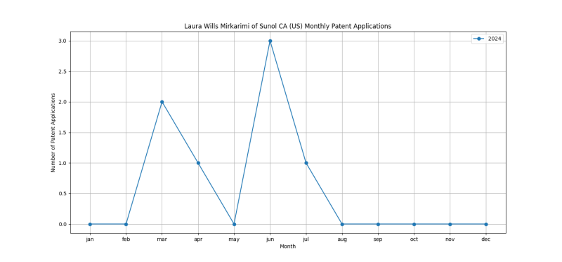
Laura Wills Mirkarimi of Sunol CA (US) is an inventor who has filed 7 patents. Their primary areas of innovation include SEMICONDUCTOR DEVICES NOT COVERED BY CLASS (4 patents), {Methods for connecting semiconductor or other solid state bodies using means for bonding being attached to, or being formed on, the surface to be connected} (4 patents), SEMICONDUCTOR DEVICES NOT COVERED BY CLASS (4 patents), and they have worked with companies such as ADEIA SEMICONDUCTOR BONDING TECHNOLOGIES INC. (7 patents). Their most frequent collaborators include (6 collaborations), (5 collaborations), (5 collaborations).
Patent Filing Activity
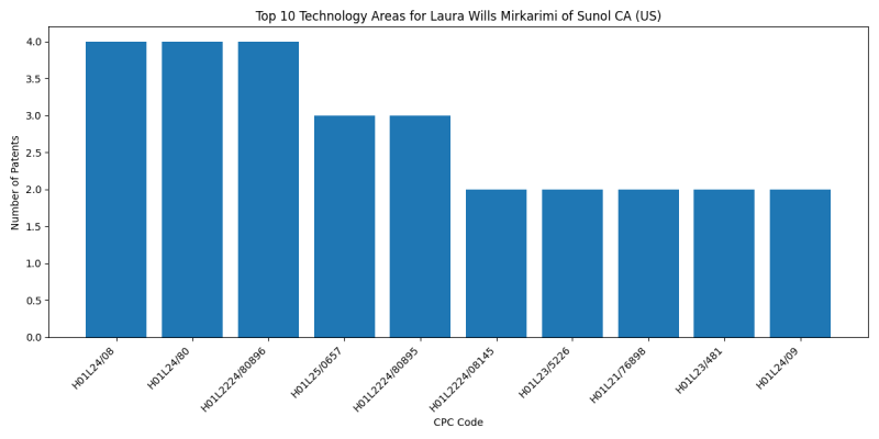
Technology Areas
List of Technology Areas
- H01L24/08 (SEMICONDUCTOR DEVICES NOT COVERED BY CLASS): 4 patents
- H01L24/80 ({Methods for connecting semiconductor or other solid state bodies using means for bonding being attached to, or being formed on, the surface to be connected}): 4 patents
- H01L2224/80896 (SEMICONDUCTOR DEVICES NOT COVERED BY CLASS): 4 patents
- H01L25/0657 (SEMICONDUCTOR DEVICES NOT COVERED BY CLASS): 3 patents
- H01L2224/80895 (SEMICONDUCTOR DEVICES NOT COVERED BY CLASS): 3 patents
- H01L2224/08145 (SEMICONDUCTOR DEVICES NOT COVERED BY CLASS): 2 patents
- H01L23/5226 (SEMICONDUCTOR DEVICES NOT COVERED BY CLASS): 2 patents
- H01L21/76898 ({formed through a semiconductor substrate}): 2 patents
- H01L23/481 (Arrangements for conducting electric current to or from the solid state body in operation, e.g. leads, terminal arrangements {; Selection of materials therefor}): 2 patents
- H01L24/09 (SEMICONDUCTOR DEVICES NOT COVERED BY CLASS): 2 patents
- H01L23/10 (SEMICONDUCTOR DEVICES NOT COVERED BY CLASS): 1 patents
- H01L21/76807 (Applying interconnections to be used for carrying current between separate components within a device {comprising conductors and dielectrics}): 1 patents
- H01L21/76816 ({Aspects relating to the layout of the pattern or to the size of vias or trenches (layout of the interconnections per se): 1 patents
- H01L2924/01029 (SEMICONDUCTOR DEVICES NOT COVERED BY CLASS): 1 patents
- H01L21/561 (SEMICONDUCTOR DEVICES NOT COVERED BY CLASS): 1 patents
- H01L23/3121 (SEMICONDUCTOR DEVICES NOT COVERED BY CLASS): 1 patents
- H01L24/97 (SEMICONDUCTOR DEVICES NOT COVERED BY CLASS): 1 patents
- H01L2224/0401 (SEMICONDUCTOR DEVICES NOT COVERED BY CLASS): 1 patents
- H01L2924/3511 (SEMICONDUCTOR DEVICES NOT COVERED BY CLASS): 1 patents
- H01L2924/35121 (SEMICONDUCTOR DEVICES NOT COVERED BY CLASS): 1 patents
- H01L2224/80948 (SEMICONDUCTOR DEVICES NOT COVERED BY CLASS): 1 patents
- H01L22/34 ({Circuits for electrically characterising or monitoring manufacturing processes, e. g. whole test die, wafers filled with test structures, on-board-devices incorporated on each die, process control monitors or pad structures thereof, devices in scribe line (switching, multiplexing, gating devices): 1 patents
- H01L21/7685 ({the layer covering a conductive structure (): 1 patents
- H01L21/76877 ({Thin films associated with contacts of capacitors}): 1 patents
- H01L23/53238 (SEMICONDUCTOR DEVICES NOT COVERED BY CLASS): 1 patents
- H01L23/53266 (SEMICONDUCTOR DEVICES NOT COVERED BY CLASS): 1 patents
- H01L23/5386 (the interconnection structure between a plurality of semiconductor chips being formed on, or in, insulating substrates ({): 1 patents
- H01L24/03 (SEMICONDUCTOR DEVICES NOT COVERED BY CLASS): 1 patents
- H01L24/05 (SEMICONDUCTOR DEVICES NOT COVERED BY CLASS): 1 patents
- H01L24/06 ({of a plurality of bonding areas}): 1 patents
- H01L25/50 ({Multistep manufacturing processes of assemblies consisting of devices, each device being of a type provided for in group): 1 patents
- H01L24/94 (SEMICONDUCTOR DEVICES NOT COVERED BY CLASS): 1 patents
- H01L2224/05147 (SEMICONDUCTOR DEVICES NOT COVERED BY CLASS): 1 patents
- H01L2224/05181 (SEMICONDUCTOR DEVICES NOT COVERED BY CLASS): 1 patents
- H01L2224/05184 (SEMICONDUCTOR DEVICES NOT COVERED BY CLASS): 1 patents
- H01L2224/08146 (SEMICONDUCTOR DEVICES NOT COVERED BY CLASS): 1 patents
- H01L2224/08057 (SEMICONDUCTOR DEVICES NOT COVERED BY CLASS): 1 patents
- H01L2224/08147 (SEMICONDUCTOR DEVICES NOT COVERED BY CLASS): 1 patents
- H01L21/76843 ({formed in openings in a dielectric}): 1 patents
- H01L21/76895 (Applying interconnections to be used for carrying current between separate components within a device {comprising conductors and dielectrics}): 1 patents
- H01L23/4824 (consisting of lead-in layers inseparably applied to the semiconductor body {(electrodes): 1 patents
- H01L24/32 (SEMICONDUCTOR DEVICES NOT COVERED BY CLASS): 1 patents
- H01L24/83 (SEMICONDUCTOR DEVICES NOT COVERED BY CLASS): 1 patents
- H01L2225/06524 (SEMICONDUCTOR DEVICES NOT COVERED BY CLASS): 1 patents
- H01L2225/06544 (SEMICONDUCTOR DEVICES NOT COVERED BY CLASS): 1 patents
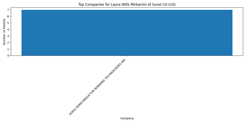
Companies
List of Companies
- ADEIA SEMICONDUCTOR BONDING TECHNOLOGIES INC.: 7 patents
Collaborators
- Rajesh Katkar of Milpitas CA (US) (6 collaborations)
- Gaius Gillman Fountain, JR. of Youngsville NC (US) (5 collaborations)
- Cyprian Emeka Uzoh of San Jose CA (US) (5 collaborations)
- Guilian Gao of San Jose CA (US) (5 collaborations)
- Belgacem Haba of Saratoga CA (US) (3 collaborations)
- Thomas Workman of San Jose CA (US) (2 collaborations)
- Bongsub Lee of Santa Clara CA (US) (2 collaborations)
- Bongsub Lee of Mountain View CA (US) (1 collaborations)
- Gabriel Z. Guevara of San Jose CA (US) (1 collaborations)
- Joy Watanabe of Campbell CA (US) (1 collaborations)
- Dominik Suwito of San Jose CA (US) (1 collaborations)
- Jeremy Alfred Theil of Mountain View CA (US) (1 collaborations)
Subcategories
This category has the following 10 subcategories, out of 10 total.
B
C
D
G
J
L
R
T
Pages in category "Laura Wills Mirkarimi of Sunol CA (US)"
This category contains only the following page.
Categories:
- Rajesh Katkar of Milpitas CA (US)
- Gaius Gillman Fountain, JR. of Youngsville NC (US)
- Cyprian Emeka Uzoh of San Jose CA (US)
- Guilian Gao of San Jose CA (US)
- Belgacem Haba of Saratoga CA (US)
- Thomas Workman of San Jose CA (US)
- Bongsub Lee of Santa Clara CA (US)
- Bongsub Lee of Mountain View CA (US)
- Gabriel Z. Guevara of San Jose CA (US)
- Joy Watanabe of Campbell CA (US)
- Dominik Suwito of San Jose CA (US)
- Jeremy Alfred Theil of Mountain View CA (US)
- Laura Wills Mirkarimi of Sunol CA (US)
- Inventors
- Inventors filing patents with ADEIA SEMICONDUCTOR BONDING TECHNOLOGIES INC.


