Difference between revisions of "Category:Yohei YAMASHITA"
Jump to navigation
Jump to search
Wikipatents (talk | contribs) (Updating Category:Yohei_YAMASHITA) |
Wikipatents (talk | contribs) (Updating Category:Yohei_YAMASHITA) |
||
| Line 2: | Line 2: | ||
=== Executive Summary === | === Executive Summary === | ||
| − | Yohei YAMASHITA is an inventor who has filed 9 patents. Their primary areas of innovation include | + | Yohei YAMASHITA is an inventor who has filed 9 patents. Their primary areas of innovation include Bombardment with radiation {( (5 patents), {Apparatus for mechanical treatment (or grinding or cutting, see the relevant groups in subclasses (2 patents), Mechanical treatment, e.g. grinding, polishing, cutting {( (2 patents), and they have worked with companies such as Tokyo Electron Limited (9 patents). Their most frequent collaborators include [[Category:Hayato TANOUE|Hayato TANOUE]] (5 collaborations), [[Category:Yasutaka MIZOMOTO|Yasutaka MIZOMOTO]] (4 collaborations), [[Category:Kento ARAKI|Kento ARAKI]] (2 collaborations). |
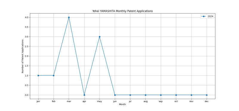
=== Patent Filing Activity === | === Patent Filing Activity === | ||
| Line 11: | Line 11: | ||
==== List of Technology Areas ==== | ==== List of Technology Areas ==== | ||
| − | * [[:Category:CPC_H01L21/268|H01L21/268]] ( | + | * [[:Category:CPC_H01L21/268|H01L21/268]] (Bombardment with radiation {(): 5 patents |
| − | * [[:Category:CPC_H01L21/67092|H01L21/67092]] ( | + | * [[:Category:CPC_H01L21/67092|H01L21/67092]] ({Apparatus for mechanical treatment (or grinding or cutting, see the relevant groups in subclasses): 2 patents |
| − | * [[:Category:CPC_H01L21/304|H01L21/304]] ( | + | * [[:Category:CPC_H01L21/304|H01L21/304]] (Mechanical treatment, e.g. grinding, polishing, cutting {(): 2 patents |
| − | * [[:Category:CPC_B23K26/361|B23K26/361]] ( | + | * [[:Category:CPC_B23K26/361|B23K26/361]] (Removing material (): 2 patents |
| − | * [[:Category:CPC_B23K2103/56|B23K2103/56]] ( | + | * [[:Category:CPC_B23K2103/56|B23K2103/56]] (SOLDERING OR UNSOLDERING; WELDING; CLADDING OR PLATING BY SOLDERING OR WELDING; CUTTING BY APPLYING HEAT LOCALLY, e.g. FLAME CUTTING; WORKING BY LASER BEAM (making metal-coated products by extruding metal): 2 patents |
| − | * [[:Category:CPC_H01L21/67115|H01L21/67115]] ( | + | * [[:Category:CPC_H01L21/67115|H01L21/67115]] ({mainly by radiation}): 2 patents |
| − | * [[:Category:CPC_H01L21/76256|H01L21/76256]] ( | + | * [[:Category:CPC_H01L21/76256|H01L21/76256]] (Dielectric regions {, e.g. EPIC dielectric isolation, LOCOS; Trench refilling techniques, SOI technology, use of channel stoppers}): 1 patents |
| − | * [[:Category:CPC_B23K26/53|B23K26/53]] ( | + | * [[:Category:CPC_B23K26/53|B23K26/53]] (SOLDERING OR UNSOLDERING; WELDING; CLADDING OR PLATING BY SOLDERING OR WELDING; CUTTING BY APPLYING HEAT LOCALLY, e.g. FLAME CUTTING; WORKING BY LASER BEAM (making metal-coated products by extruding metal): 1 patents |
| − | * [[:Category:CPC_H01L21/02164|H01L21/02164]] ( | + | * [[:Category:CPC_H01L21/02164|H01L21/02164]] ({the material being a silicon oxide, e.g. SiO): 1 patents |
| − | * [[:Category:CPC_H01L21/02238|H01L21/02238]] ( | + | * [[:Category:CPC_H01L21/02238|H01L21/02238]] ({the layer being a laminate, i.e. composed of sublayers, e.g. stacks of alternating high-k metal oxides (adhesion layers or buffer layers): 1 patents |
| − | * [[:Category:CPC_B23K2101/40|B23K2101/40]] ( | + | * [[:Category:CPC_B23K2101/40|B23K2101/40]] (SOLDERING OR UNSOLDERING; WELDING; CLADDING OR PLATING BY SOLDERING OR WELDING; CUTTING BY APPLYING HEAT LOCALLY, e.g. FLAME CUTTING; WORKING BY LASER BEAM (making metal-coated products by extruding metal): 1 patents |
| − | * [[:Category:CPC_H01L25/50|H01L25/50]] ( | + | * [[:Category:CPC_H01L25/50|H01L25/50]] ({Multistep manufacturing processes of assemblies consisting of devices, each device being of a type provided for in group): 1 patents |
| − | * [[:Category:CPC_H01L21/67132|H01L21/67132]] ( | + | * [[:Category:CPC_H01L21/67132|H01L21/67132]] ({Apparatus for placing on an insulating substrate, e.g. tape}): 1 patents |
| − | * [[:Category:CPC_H01L21/6835|H01L21/6835]] ( | + | * [[:Category:CPC_H01L21/6835|H01L21/6835]] ({using temporarily an auxiliary support}): 1 patents |
| − | * [[:Category:CPC_H01L25/0652|H01L25/0652]] ( | + | * [[:Category:CPC_H01L25/0652|H01L25/0652]] (SEMICONDUCTOR DEVICES NOT COVERED BY CLASS): 1 patents |
| − | * [[:Category:CPC_H01L2221/68309|H01L2221/68309]] ( | + | * [[:Category:CPC_H01L2221/68309|H01L2221/68309]] (SEMICONDUCTOR DEVICES NOT COVERED BY CLASS): 1 patents |
| − | * [[:Category:CPC_H01L2221/68327|H01L2221/68327]] ( | + | * [[:Category:CPC_H01L2221/68327|H01L2221/68327]] (SEMICONDUCTOR DEVICES NOT COVERED BY CLASS): 1 patents |
| − | * [[:Category:CPC_H01L2221/68368|H01L2221/68368]] ( | + | * [[:Category:CPC_H01L2221/68368|H01L2221/68368]] (SEMICONDUCTOR DEVICES NOT COVERED BY CLASS): 1 patents |
| − | * [[:Category:CPC_H01L2221/68381|H01L2221/68381]] ( | + | * [[:Category:CPC_H01L2221/68381|H01L2221/68381]] (SEMICONDUCTOR DEVICES NOT COVERED BY CLASS): 1 patents |
| − | * [[:Category:CPC_B23K26/352|B23K26/352]] ( | + | * [[:Category:CPC_B23K26/352|B23K26/352]] (for surface treatment): 1 patents |
| − | * [[:Category:CPC_B23K26/082|B23K26/082]] ( | + | * [[:Category:CPC_B23K26/082|B23K26/082]] (Devices involving relative movement between laser beam and workpiece): 1 patents |
| − | * [[:Category:CPC_H01L21/6831|H01L21/6831]] ( | + | * [[:Category:CPC_H01L21/6831|H01L21/6831]] (for supporting or gripping (for conveying): 1 patents |
| − | * [[:Category:CPC_B23K26/0823|B23K26/0823]] ( | + | * [[:Category:CPC_B23K26/0823|B23K26/0823]] (Devices involving relative movement between laser beam and workpiece): 1 patents |
| − | * [[:Category:CPC_B23K26/083|B23K26/083]] ( | + | * [[:Category:CPC_B23K26/083|B23K26/083]] (Devices involving relative movement between laser beam and workpiece): 1 patents |
| − | * [[:Category:CPC_B23K26/18|B23K26/18]] ( | + | * [[:Category:CPC_B23K26/18|B23K26/18]] (using absorbing layers on the workpiece, e.g. for marking or protecting purposes): 1 patents |
| − | * [[:Category:CPC_B23K26/402|B23K26/402]] ( | + | * [[:Category:CPC_B23K26/402|B23K26/402]] (involving non-metallic material, e.g. isolators): 1 patents |
| − | * [[:Category:CPC_H01L21/447|H01L21/447]] ( | + | * [[:Category:CPC_H01L21/447|H01L21/447]] (involving the application of pressure, e.g. thermo-compression bonding): 1 patents |
| − | * [[:Category:CPC_H01L21/67144|H01L21/67144]] ( | + | * [[:Category:CPC_H01L21/67144|H01L21/67144]] ({Apparatus for mounting on conductive members, e.g. leadframes or conductors on insulating substrates}): 1 patents |
| − | * [[:Category:CPC_H01L21/78|H01L21/78]] ( | + | * [[:Category:CPC_H01L21/78|H01L21/78]] (with subsequent division of the substrate into plural individual devices (cutting to change the surface-physical characteristics or shape of semiconductor bodies): 1 patents |
| − | * [[:Category:CPC_H01L21/6836|H01L21/6836]] ( | + | * [[:Category:CPC_H01L21/6836|H01L21/6836]] ({Wafer tapes, e.g. grinding or dicing support tapes (adhesive tapes in general): 1 patents |
| − | * [[:Category:CPC_H01L21/02035|H01L21/02035]] ( | + | * [[:Category:CPC_H01L21/02035|H01L21/02035]] ({Shaping}): 1 patents |
| − | * [[:Category:CPC_H01L21/67207|H01L21/67207]] ( | + | * [[:Category:CPC_H01L21/67207|H01L21/67207]] (Apparatus specially adapted for handling semiconductor or electric solid state devices during manufacture or treatment thereof; Apparatus specially adapted for handling wafers during manufacture or treatment of semiconductor or electric solid state devices or components {; Apparatus not specifically provided for elsewhere (processes per se): 1 patents |
| − | * [[:Category:CPC_H01L21/67288|H01L21/67288]] ( | + | * [[:Category:CPC_H01L21/67288|H01L21/67288]] (Apparatus specially adapted for handling semiconductor or electric solid state devices during manufacture or treatment thereof; Apparatus specially adapted for handling wafers during manufacture or treatment of semiconductor or electric solid state devices or components {; Apparatus not specifically provided for elsewhere (processes per se): 1 patents |
| − | * [[:Category:CPC_H01L21/02013|H01L21/02013]] ( | + | * [[:Category:CPC_H01L21/02013|H01L21/02013]] ({Grinding, lapping}): 1 patents |
| − | * [[:Category:CPC_H01L21/02019|H01L21/02019]] ( | + | * [[:Category:CPC_H01L21/02019|H01L21/02019]] ({Chemical etching}): 1 patents |
| − | * [[:Category:CPC_H01L22/20|H01L22/20]] ( | + | * [[:Category:CPC_H01L22/20|H01L22/20]] ({Sequence of activities consisting of a plurality of measurements, corrections, marking or sorting steps}): 1 patents |
| − | * [[:Category:CPC_B23K26/032|B23K26/032]] ( | + | * [[:Category:CPC_B23K26/032|B23K26/032]] (SOLDERING OR UNSOLDERING; WELDING; CLADDING OR PLATING BY SOLDERING OR WELDING; CUTTING BY APPLYING HEAT LOCALLY, e.g. FLAME CUTTING; WORKING BY LASER BEAM (making metal-coated products by extruding metal): 1 patents |
| − | * [[:Category:CPC_B24B7/22|B24B7/22]] ( | + | * [[:Category:CPC_B24B7/22|B24B7/22]] (MACHINES, DEVICES, OR PROCESSES FOR GRINDING OR POLISHING (grinding of gear teeth): 1 patents |
=== Companies === | === Companies === | ||
Latest revision as of 09:06, 19 July 2024
Contents
Yohei YAMASHITA
Executive Summary
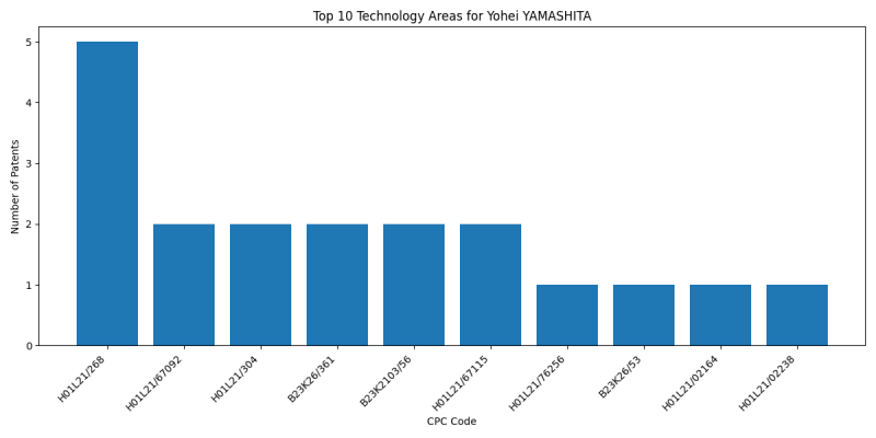
Yohei YAMASHITA is an inventor who has filed 9 patents. Their primary areas of innovation include Bombardment with radiation {( (5 patents), {Apparatus for mechanical treatment (or grinding or cutting, see the relevant groups in subclasses (2 patents), Mechanical treatment, e.g. grinding, polishing, cutting {( (2 patents), and they have worked with companies such as Tokyo Electron Limited (9 patents). Their most frequent collaborators include (5 collaborations), (4 collaborations), (2 collaborations).
Patent Filing Activity
Technology Areas
List of Technology Areas
- H01L21/268 (Bombardment with radiation {(): 5 patents
- H01L21/67092 ({Apparatus for mechanical treatment (or grinding or cutting, see the relevant groups in subclasses): 2 patents
- H01L21/304 (Mechanical treatment, e.g. grinding, polishing, cutting {(): 2 patents
- B23K26/361 (Removing material (): 2 patents
- B23K2103/56 (SOLDERING OR UNSOLDERING; WELDING; CLADDING OR PLATING BY SOLDERING OR WELDING; CUTTING BY APPLYING HEAT LOCALLY, e.g. FLAME CUTTING; WORKING BY LASER BEAM (making metal-coated products by extruding metal): 2 patents
- H01L21/67115 ({mainly by radiation}): 2 patents
- H01L21/76256 (Dielectric regions {, e.g. EPIC dielectric isolation, LOCOS; Trench refilling techniques, SOI technology, use of channel stoppers}): 1 patents
- B23K26/53 (SOLDERING OR UNSOLDERING; WELDING; CLADDING OR PLATING BY SOLDERING OR WELDING; CUTTING BY APPLYING HEAT LOCALLY, e.g. FLAME CUTTING; WORKING BY LASER BEAM (making metal-coated products by extruding metal): 1 patents
- H01L21/02164 ({the material being a silicon oxide, e.g. SiO): 1 patents
- H01L21/02238 ({the layer being a laminate, i.e. composed of sublayers, e.g. stacks of alternating high-k metal oxides (adhesion layers or buffer layers): 1 patents
- B23K2101/40 (SOLDERING OR UNSOLDERING; WELDING; CLADDING OR PLATING BY SOLDERING OR WELDING; CUTTING BY APPLYING HEAT LOCALLY, e.g. FLAME CUTTING; WORKING BY LASER BEAM (making metal-coated products by extruding metal): 1 patents
- H01L25/50 ({Multistep manufacturing processes of assemblies consisting of devices, each device being of a type provided for in group): 1 patents
- H01L21/67132 ({Apparatus for placing on an insulating substrate, e.g. tape}): 1 patents
- H01L21/6835 ({using temporarily an auxiliary support}): 1 patents
- H01L25/0652 (SEMICONDUCTOR DEVICES NOT COVERED BY CLASS): 1 patents
- H01L2221/68309 (SEMICONDUCTOR DEVICES NOT COVERED BY CLASS): 1 patents
- H01L2221/68327 (SEMICONDUCTOR DEVICES NOT COVERED BY CLASS): 1 patents
- H01L2221/68368 (SEMICONDUCTOR DEVICES NOT COVERED BY CLASS): 1 patents
- H01L2221/68381 (SEMICONDUCTOR DEVICES NOT COVERED BY CLASS): 1 patents
- B23K26/352 (for surface treatment): 1 patents
- B23K26/082 (Devices involving relative movement between laser beam and workpiece): 1 patents
- H01L21/6831 (for supporting or gripping (for conveying): 1 patents
- B23K26/0823 (Devices involving relative movement between laser beam and workpiece): 1 patents
- B23K26/083 (Devices involving relative movement between laser beam and workpiece): 1 patents
- B23K26/18 (using absorbing layers on the workpiece, e.g. for marking or protecting purposes): 1 patents
- B23K26/402 (involving non-metallic material, e.g. isolators): 1 patents
- H01L21/447 (involving the application of pressure, e.g. thermo-compression bonding): 1 patents
- H01L21/67144 ({Apparatus for mounting on conductive members, e.g. leadframes or conductors on insulating substrates}): 1 patents
- H01L21/78 (with subsequent division of the substrate into plural individual devices (cutting to change the surface-physical characteristics or shape of semiconductor bodies): 1 patents
- H01L21/6836 ({Wafer tapes, e.g. grinding or dicing support tapes (adhesive tapes in general): 1 patents
- H01L21/02035 ({Shaping}): 1 patents
- H01L21/67207 (Apparatus specially adapted for handling semiconductor or electric solid state devices during manufacture or treatment thereof; Apparatus specially adapted for handling wafers during manufacture or treatment of semiconductor or electric solid state devices or components {; Apparatus not specifically provided for elsewhere (processes per se): 1 patents
- H01L21/67288 (Apparatus specially adapted for handling semiconductor or electric solid state devices during manufacture or treatment thereof; Apparatus specially adapted for handling wafers during manufacture or treatment of semiconductor or electric solid state devices or components {; Apparatus not specifically provided for elsewhere (processes per se): 1 patents
- H01L21/02013 ({Grinding, lapping}): 1 patents
- H01L21/02019 ({Chemical etching}): 1 patents
- H01L22/20 ({Sequence of activities consisting of a plurality of measurements, corrections, marking or sorting steps}): 1 patents
- B23K26/032 (SOLDERING OR UNSOLDERING; WELDING; CLADDING OR PLATING BY SOLDERING OR WELDING; CUTTING BY APPLYING HEAT LOCALLY, e.g. FLAME CUTTING; WORKING BY LASER BEAM (making metal-coated products by extruding metal): 1 patents
- B24B7/22 (MACHINES, DEVICES, OR PROCESSES FOR GRINDING OR POLISHING (grinding of gear teeth): 1 patents
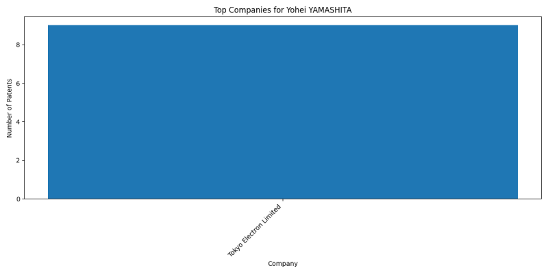
Companies
List of Companies
- Tokyo Electron Limited: 9 patents
Collaborators
- Hayato TANOUE (5 collaborations)
- Yasutaka MIZOMOTO (4 collaborations)
- Kento ARAKI (2 collaborations)
- Gousuke SHIRAISHI (2 collaborations)
- Yoshihiro KAWAGUCHI (1 collaborations)
- Yoshihisa MATSUBARA (1 collaborations)
- Yoshihiro TSUTSUMI (1 collaborations)
- Susumu HAYAKAWA (1 collaborations)


